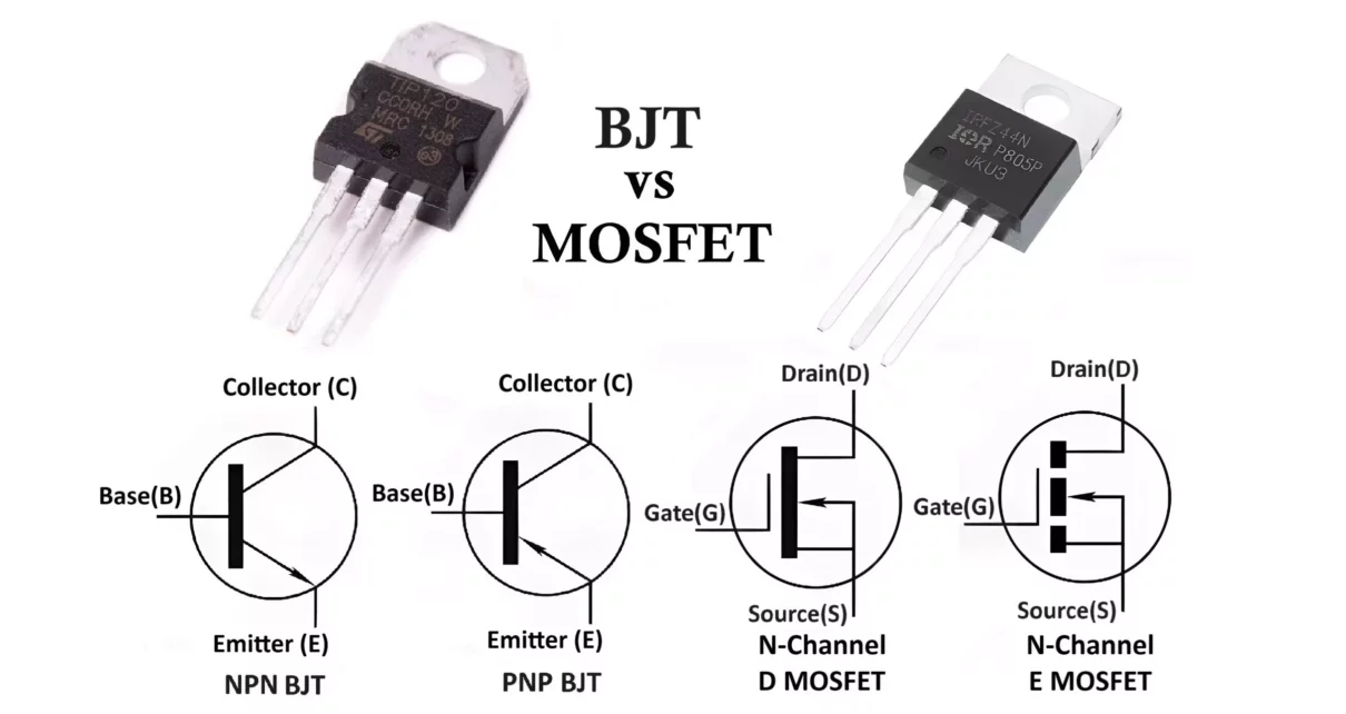
Let’s understand the Difference Between BJT and MOSFET. Bipolar Junction Transistors (BJTs) and Metal-Oxide-Semiconductor Field-Effect Transistors (MOSFETs) are two fundamental types of transistors used in electronic circuits. They have several key differences in terms of their structure, operation, and applications:
What is BJT?
A Bipolar Junction Transistor (BJT) is a semiconductor device used for amplification and switching. BJTs are current-controlled devices where the output current is controlled by the input base current. They have three terminals: emitter, base, and collector. BJTs come in two types: NPN and PNP, differing in the type of charge carriers (electrons for NPN and holes for PNP).
Working Principle of BJT:
The BJT operates by using voltage between the base and emitter to control the current flow through the collector. In a common emitter configuration, the input voltage controls the base current, which in turn controls the output current at the collector.
Type of BJT:
There are two types of Bipolar Junction Transistors (BJT) NPN and PNP. They involve three layers of semiconductor material, forming two PN junctions. These layers are arranged in either an NPN or PNP configuration, depending on the type of BJT.

NPN Transistor Construction:
Layers: There are three layers of NPN transistor.
Emitter (N-type): Heavily doped with donor impurities, providing a high concentration of free electrons.
The high doping level ensures a large number of carriers are injected into the base when the emitter-base junction is forward-biased.
Base (P-type): Lightly doped with acceptor impurities, resulting in a thin layer with a moderate concentration of holes.
Its primary function is to pass majority carriers from the emitter to the collector with minimal recombination.
The thinness of the base is critical to allow most carriers to diffuse through to the collector.
Collector (N-type): Moderately doped, thicker compared to the emitter to handle the majority of the collected current.
It is designed to handle higher voltages and dissipate power.
Junctions:
Emitter-Base Junction (EBJ): A PN junction between the emitter and the base.
Collector-Base Junction (CBJ): A PN junction between the collector and the base.
PNP Transistor Construction:
Layers: There are three layers of PNP transistor.
Emitter (P-type): Heavily doped with acceptor impurities, providing a high concentration of holes.
Base (N-type): Lightly doped with donor impurities, resulting in a thin layer with a moderate concentration of electrons.
Collector (P-type): Moderately doped, thicker compared to the emitter to handle the majority of the collected current.
Junctions:
Emitter-Base Junction (EBJ): A PN junction between the emitter and the base.
Collector-Base Junction (CBJ): A PN junction between the collector and the base.
Terminals:
Emitter (E): Connected to the heavily doped (N or P)-type region.
Base (B): Connected to the lightly doped (P or N)-type region.
Collector (C): Connected to the moderately doped (N or P)-type region.

Working of BJT:
Forward Active Mode (NPN Example):
The emitter-base junction is forward-biased, allowing electrons to flow from the emitter into the base.
The base-collector junction is reverse-biased, creating an electric field that sweeps the electrons from the base into the collector.
Most of the electrons injected into the base from the emitter diffuse through the thin base and are collected by the collector.
A small base current controls a much larger collector current, providing current amplification.
Operation Regions:
Both BJT and MOSFET have three operating regions.
Active Region: Emitter-base junction is forward-biased, collector-base junction is reverse-biased. The transistor acts as an amplifier.
Saturation Region: Both junctions are forward-biased. The transistor acts as a closed switch.
Cutoff Region: Both junctions are reverse-biased. The transistor acts as an open switch.
Advantages and Disadvantages of BJT:
Advantages of BJT:
High Gain: BJTs have high current gain, making them suitable for amplifying weak signals.
High Frequency Response: BJTs have a wide frequency response, meaning they can operate efficiently at high frequencies, making them suitable for RF (radio frequency) applications.
Better Linearity: BJTs offer better linearity compared to MOSFETs, making them suitable for analog signal amplification where linear amplification is required.
High Voltage Operation: BJTs can handle high voltage levels, which makes them ideal for power amplification and switching applications.
Simplicity in Biasing: Biasing a BJT is relatively straightforward, and they can be easily implemented in a variety of circuit designs.
Thermal Runaway Protection: BJTs have built-in thermal runaway protection, which can be advantageous in applications where temperature stability is critical.
Disadvantages of BJT:
High Power Consumption: BJTs consume more power due to their higher base current requirements, making them less efficient compared to MOSFETs, especially in low-power applications.
Lower Input Impedance: BJTs have lower input impedance, which can lead to loading effects in certain applications, requiring additional circuit complexity to manage impedance matching.
Slower Switching Speed: BJTs generally have slower switching speeds compared to MOSFETs, making them less suitable for high-speed switching applications.
Thermal Stability Issues: BJTs are more sensitive to temperature changes, which can affect their performance and reliability over time, requiring additional thermal management in circuit design.
Larger Size: BJTs are typically larger in size compared to MOSFETs, making them less ideal for compact or miniaturized circuit designs.
Noise Generation: BJTs tend to generate more noise compared to MOSFETs, which can be a disadvantage in low-noise signal processing applications.
What is MOSFET?
A Metal Oxide Semiconductor Field Effect Transistor (MOSFET) is a type of FET that is voltage-controlled. It has three terminals: gate, source, and drain. MOSFETs are available in four types: N-channel and P-channel, each with enhancement and depletion modes.
Working Principle of MOSFET:
The operation of a MOSFET depends on the metal oxide capacitor. By applying a voltage to the gate, an electric field is created, altering the conductivity of the channel between the source and drain. This allows for the control of the current flow.
Types of MOSFET:
The construction of a Metal-Oxide-Semiconductor Field-Effect Transistor (MOSFET) involves several key components, including a semiconductor substrate, a gate, a source, and a drain, along with an insulating oxide layer. MOSFETs come in two types: n-channel and p-channel. With two configurations Enhancement Mode and Depletion Mode.

N-Channel MOSFET:
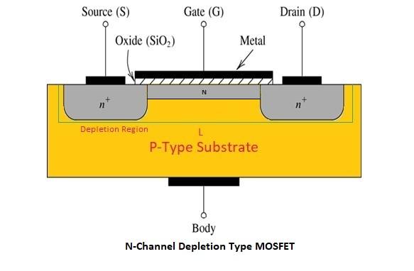
Substrate:
Type: Usually a p-type silicon substrate for n-channel MOSFETs.
Function: Acts as the body of the transistor, providing a platform for the formation of the source and drain regions.
Source and Drain:
Doping: The source and drain regions are heavily doped with n-type impurities (n+ regions), creating areas with a high concentration of free electrons.
Location: These regions are placed at opposite ends of the transistor and are connected to the external circuit.
Gate:
Material: Typically made of polysilicon or metal.
Position: Located above the channel region, separated from the substrate by a thin insulating layer of silicon dioxide (SiO2).
Insulating Layer (Gate Oxide):
Material: Silicon dioxide (SiO2).
Function: Insulates the gate from the underlying semiconductor material, allowing the gate to control the channel current without direct electrical contact.
Channel:
Formation: The channel forms in the substrate beneath the gate when a sufficient voltage is applied to the gate.
Type: For an n-channel MOSFET, the channel consists of electrons in the p-type substrate.
P-Channel MOSFET:
Substrate:
Type: Usually an n-type silicon substrate for p-channel MOSFETs.
Function: Acts as the body of the transistor, providing a platform for the formation of the source and drain regions.
Source and Drain:
Doping: The source and drain regions are heavily doped with p-type impurities (p+ regions), creating areas with a high concentration of holes.
Location: These regions are placed at opposite ends of the transistor and are connected to the external circuit.
Gate:
Material: Typically made of polysilicon or metal.
Position: Located above the channel region, separated from the substrate by a thin insulating layer of silicon dioxide (SiO2).
Insulating Layer (Gate Oxide):
Material: Silicon dioxide (SiO2).
Function: Insulates the gate from the underlying semiconductor material, allowing the gate to control the channel current without direct electrical contact.
Channel:
Formation: The channel forms in the substrate beneath the gate when a sufficient voltage is applied to the gate.
Type: For a p-channel MOSFET, the channel consists of holes in the n-type substrate.
Detailed Construction of MOSFET:
Source Region:
Heavily doped n-type (n+ for n-channel MOSFET) or p-type (p+ for p-channel MOSFET).
Provides the majority charge carriers (electrons for n-channel, holes for p-channel).
Drain Region:
Heavily doped n-type (n+ for n-channel MOSFET) or p-type (p+ for p-channel MOSFET).
Collects the charge carriers from the channel.
Gate Region:
Positioned above the channel with an insulating silicon dioxide layer between the gate and the substrate.
Controls the formation of the channel by applying a voltage.
Channel Formation:
For an n-channel MOSFET, when a positive voltage is applied to the gate, it attracts electrons to the surface of the p-type substrate, creating a conductive n-type channel between the source and drain.
For a p-channel MOSFET, when a negative voltage is applied to the gate, it attracts holes to the surface of the n-type substrate, creating a conductive p-type channel between the source and drain.
Working of MOSFET:
Enhancement Mode (N-Channel Example):
Off State: When the gate-source voltage (V_GS) is zero or negative, the MOSFET is off, and no current flows between the source and drain.
On State: When a positive V_GS is applied, an electric field is created, attracting electrons to form a conductive channel between the source and drain, allowing current to flow.
Depletion Mode:
Off State: For depletion-mode MOSFETs, a channel exists even when V_GS is zero. Applying a voltage of opposite polarity can deplete the channel of carriers, turning the MOSFET off.
Advantages and Disadvantages of MOSFET:
Advantages of MOSFETs:
High Switching Speed: MOSFETs can switch on and off very quickly, making them ideal for high-frequency applications.
Low Power Consumption: They consume less power due to high input impedance, resulting in minimal gate current.
High Input Impedance: The high input impedance makes them suitable for voltage-driven applications and results in minimal power loss at the control terminal.
Thermal Stability: MOSFETs have a positive temperature coefficient, which means they are less prone to thermal runaway and can handle higher power levels more reliably.
Small Size: MOSFETs can be made very small, allowing for high-density integration in chips, which is crucial for modern electronics like smartphones and computers.
Disadvantages of MOSFETs:
Sensitive to Static Discharge: MOSFETs are highly sensitive to static electricity, which can damage them if proper handling precautions are not taken.
Complex Manufacturing: The fabrication process of MOSFETs can be more complex compared to BJTs, resulting in higher production costs.
Overvoltage Vulnerability: MOSFETs can be easily damaged by overvoltage conditions, requiring careful circuit design to protect them.
Short Lifespan in Some Applications: In certain applications, particularly those involving high-stress conditions, MOSFETs might have a shorter lifespan compared to other types of transistors.
Calibration Requirement: Frequent calibration may be required for precise operation, particularly in sensitive applications.
Difference between BJT and MOSFET:
| Characteristic | BJT | MOSFET |
|---|---|---|
| Control Mechanism | Current-controlled | Voltage-controlled |
| Charge Carriers | Electrons (NPN), Holes (PNP) | Majority carriers (N or P type) |
| Temperature Coefficient | Negative | Positive |
| Input Impedance | Low | High |
| Output Control | Base current | Gate voltage |
| Cost | Generally cheaper | Generally more expensive |
| Sensitivity to ESD | Less | More |
| Current Gain | Low and not stable | High and stable |
| Switching Speed | Slower | Faster |
| Power Consumption | Higher | Lower |
| Size | Larger | Smaller |
| Noise Immunity | Lower | Higher |
| Applications | Low current | High power |

Applications of BJT and MOSFET:
Bipolar Junction Transistor (BJT):
Analog Circuits: Amplifiers, linear regulators.
Switching Applications: Low-speed switches, motor drivers.
Signal Processing: Used where high gain is required.
Metal-Oxide-Semiconductor Field-Effect Transistor (MOSFET):
Digital Circuits: Logic gates, microprocessors, memory devices.
High-Frequency Applications: RF amplifiers, fast-switching circuits.
Power Applications: Power supplies, DC-DC converters, motor controllers.
Summary of Key Differences Between BJT and MOSFET:
- Control Mechanism: BJTs are current-controlled devices, while MOSFETs are voltage-controlled devices.
- Carrier Type: BJTs are bipolar, using both electrons and holes, whereas MOSFETs are unipolar, using either electrons (n-channel) or holes (p-channel).
- Input Impedance: BJTs have low input impedance; MOSFETs have high input impedance.
- Switching Speed: BJTs are generally slower than MOSFETs.
- Power Efficiency: MOSFETs are typically more power-efficient, especially in high-speed and high-frequency applications.
The choice between BJT and MOSFET depends on specific application requirements. For high-speed, low-power applications, MOSFETs are generally better. For applications needing high current and low voltage, BJTs may be more suitable. Evaluating factors like power dissipation, switching speed, thermal stability, and cost is crucial in making the right choice.
