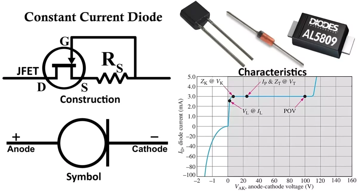
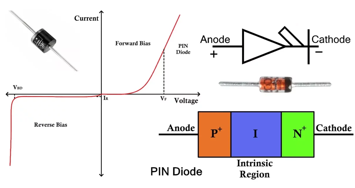
The tunnel diode, also known as the Esaki diode, is a type of semiconductor diode that exhibits a unique behavior due to quantum mechanical tunneling. Leo Esaki invented the tunnel diode in 1957, and he received the Nobel Prize in Physics for it in 1973. Its negative resistance region in the current-voltage (I-V) characteristics makes […]
Working of Diode
PIN Diode Symbol, Construction, Working & Applications
In this article, we will explore the PIN diode in detail, covering its symbol, construction, VI characteristics, working principle, advantages, disadvantages, and applications. A PIN diode is a type of semiconductor device that is widely used in RF and microwave applications. The name “PIN” comes from the structure of the diode, which consists of three […]
Schottky Diode Symbol, Construction, Working & Applications
The Schottky diode, a significant component in modern electronics, is known for its low forward voltage drop and fast switching speed. It finds extensive use in applications requiring high efficiency and low power loss. This article provides an in-depth explanation of the Schottky diode, covering its symbol, construction, VI characteristics, working, advantages, disadvantages, and applications. […]
Varactor Diode Symbol, Construction, Working & Applications
A varactor diode is a specialized semiconductor device widely used in electronics to utilize its property of variable capacitance. By understanding its symbol, construction, working principles, and applications, engineers can design systems that take advantage of its unique characteristics. This article provides a detailed overview of the varactor diode. Varactor Diode Symbol The symbol of […]
Step Recovery Diode Symbol, Construction, Working & Applications
A Step Recovery Diode (SRD) is a special type of semiconductor diode also called as snap-off diode and charge storage diode. Step recovery diodes are having a different style of doping, it is not like a normal PN junction diode. The operation of SRD is based on the principle of storing and releasing charge during […]
Shockley Diode Symbol Construction, Working and Applications
You can see Shockley diode symbol it is a four-layer (P-N-P-N) semiconductor device. Like pn junction diode It conducts in forward bias and stops conducting in reverse bias. The main difference between a conventional diode and a Shockley diode is, it starts conducting when the forward voltage crosses its breakdown voltage. It is an active component. It […]