The tunnel diode, also known as the Esaki diode, is a type of semiconductor diode that exhibits a unique behavior due to quantum mechanical tunneling. Leo Esaki invented the tunnel diode in 1957, and he received the Nobel Prize in Physics for it in 1973. Its negative resistance region in the current-voltage (I-V) characteristics makes the tunnel diode useful in various high-frequency applications. This article will delve into the symbol, construction, working principle, VI characteristics, advantages, disadvantages, and applications of the tunnel diode.
Tunnel Diode Symbol
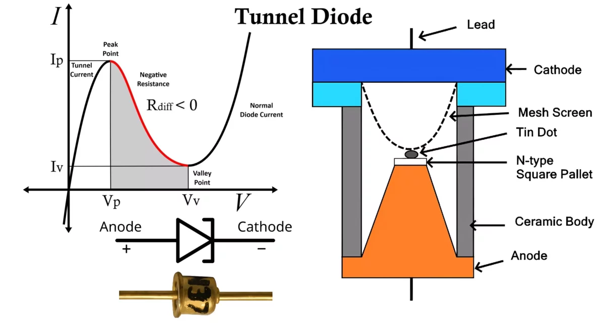
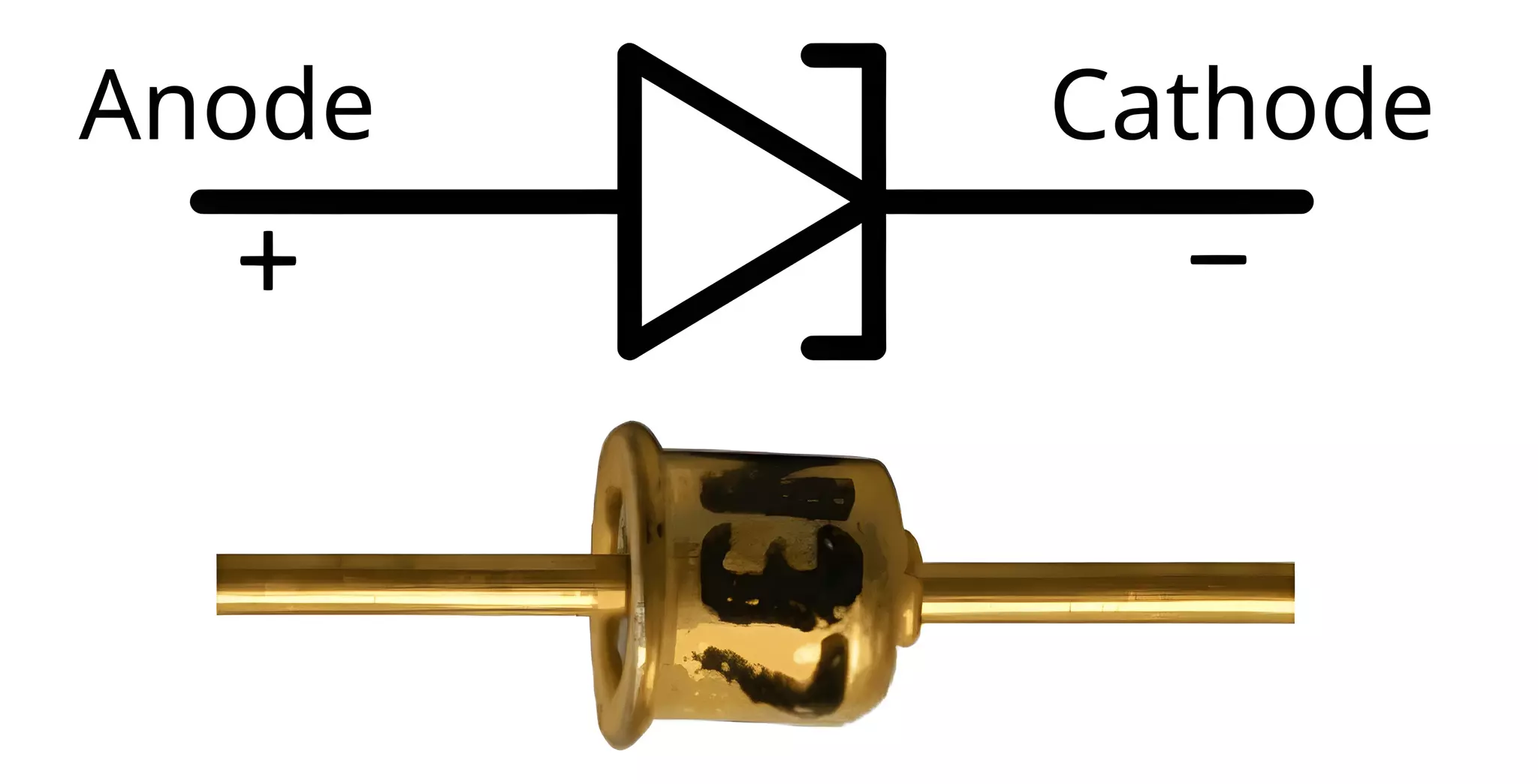
The symbol of a tunnel diode is similar to that of a standard PN junction diode but with a slight modification to represent its unique characteristics. The symbol consists of a triangle representing the anode (P-type material) and a bar representing the cathode (N-type material). The triangle is often depicted with a small gap or a series of lines near the junction to indicate the tunneling effect.
Construction of Tunnel Diode
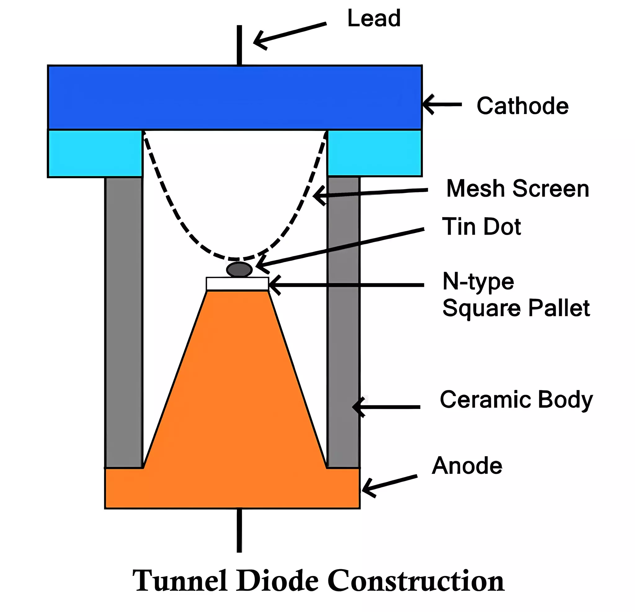
The tunnel diode is constructed using heavily doped P-type and N-type semiconductor materials. The doping concentration is typically in the range of 1019 to 1020 atoms per cubic centimeter, which is much higher than that of a conventional diode. This heavy doping results in a very narrow depletion region, typically on the order of 10 nanometers.
A tunnel diode consists of the following key elements:
- Heavily Doped p-n Junction
- The p-region and n-region are extremely heavily doped (about 1000 times more than a normal diode).
- This results in a very narrow depletion region (about 10 nm) which allows quantum tunneling to occur.
- Ohmic Contacts
- Metal contacts are attached to both p and n regions for electrical connections.
- These contacts have very low resistance to minimize losses.
- Substrate
- A semiconductor wafer (typically GaAs or Ge) serves as the base material for the diode.
Construction Process
- Selecting the Semiconductor Material
Manufacturers choose Gallium Arsenide (GaAs), Germanium (Ge), or Silicon (Si) as the base material and prefer GaAs for high-speed applications due to its superior electron mobility. - Heavily Doping the p and n Regions
The process dopes the p-region with an acceptor impurity (e.g., Boron) and the n-region with a donor impurity (e.g., Phosphorus). This heavy doping level, around 10¹⁹ to 10²⁰ carriers/cm³, creates a very narrow depletion layer. - Forming the p-n Junction
The fabrication process diffuses or grows the highly doped p and n regions using epitaxial growth techniques. The narrow depletion layer allows electrons to tunnel through the junction. - Adding Metal Contacts
The process deposits ohmic metal contacts (e.g., gold, platinum) onto the p and n sides using photolithography, ensuring efficient current flow with minimal resistance. - Encapsulating and Packaging the Device
A protective encapsulation layer prevents contamination. The device is then mounted on a ceramic or plastic package with wire leads for external connections.
Working of Tunnel Diode
The working principle of a tunnel diode is based on the quantum mechanical phenomenon known as tunneling. Tunneling occurs when electrons pass through a potential barrier that they classically should not be able to surmount due to their energy levels. In a tunnel diode, the heavy doping creates a very narrow depletion region, allowing electrons to tunnel through the junction even at low forward bias voltages.
Forward Bias Operation
- Low Forward Bias (0V to Vp): As the voltage increases from 0V to the peak voltage (Vp), electrons in the conduction band of the N-type material align with empty states in the valence band of the P-type material. This alignment allows electrons to tunnel through the narrow depletion region, resulting in a rapid increase in current.
- Peak Voltage (Vp): At the peak voltage Vp, the tunneling current reaches its maximum value, known as the peak current Ip.
- Negative Resistance Region (Vp to Vv): As the forward bias voltage increases beyond Vp, the alignment between the conduction band of the N-type material and the valence band of the P-type material begins to deteriorate. This misalignment reduces the tunneling current, leading to a decrease in current with increasing voltage. This region is known as the negative resistance region, where the diode exhibits a negative differential resistance (NDR).
- Valley Voltage (Vv): At the valley voltage Vv, the tunneling current reaches its minimum value, known as the valley current Iv.
- High Forward Bias (Beyond Vv): As the forward bias voltage increases beyond Vv, the diode behaves like a conventional PN junction diode, with the current increasing exponentially due to thermionic emission.
Reverse Bias Operation
In reverse bias, the tunnel diode behaves similarly to a conventional diode, with a small reverse saturation current flowing due to minority carriers. However, the heavy doping results in a low breakdown voltage, making the tunnel diode unsuitable for high reverse voltage applications.
VI Characteristics of Tunnel Diode
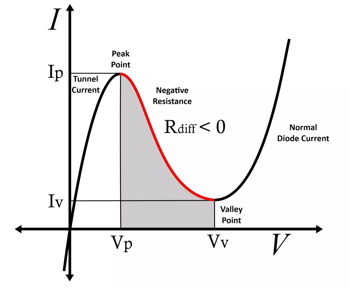
The current-voltage (I-V) characteristics of a tunnel diode are unique and differ significantly from those of a conventional diode. The I-V curve can be divided into several regions:
- Region 1 (0V to Vp): In this region, the current increases rapidly with increasing forward bias voltage due to tunneling. The slope of the curve is positive, indicating a positive resistance.
- Region 2 (Vp to Vv): This is the negative resistance region, where the current decreases with increasing voltage. The slope of the curve is negative, indicating negative differential resistance (Rdiff).
- Region 3 (Beyond Vv): In this region, the diode behaves like a conventional PN junction diode, with the current increasing exponentially with increasing voltage.
- Reverse Bias Region: The reverse bias region is characterized by a small reverse saturation current, which increases slightly with increasing reverse bias voltage.
The unique shape of the I-V curve, particularly the negative resistance region, makes the tunnel diode useful in various high-frequency applications.
RLC Equivalent Circuit of Tunnel Diode
The equivalent circuit of a tunnel diode represents its electrical behavior using passive components like resistors, capacitors, and inductors. Due to the unique negative resistance characteristic of the tunnel diode, its equivalent circuit is slightly different from regular diodes.
The equivalent circuit consists of the following components:
- Negative Resistance (-Ro): Represents the negative resistance region in the I-V characteristic of the tunnel diode.
- Junction Capacitance (Co): Represents the diode’s capacitance due to the depletion region.
- Series Resistance (Rs): Represents the resistance of the leads and contacts.
- Parasitic Inductance (Ls): Represents the inductance of the diode’s package and wiring.
Simplified Small-Signal Equivalent Circuit
For small-signal analysis, the tunnel diode can be modeled as:
- A negative resistance -Ro in parallel with the junction capacitance Co.
- In series with a small resistance Rs and parasitic inductance Ls.
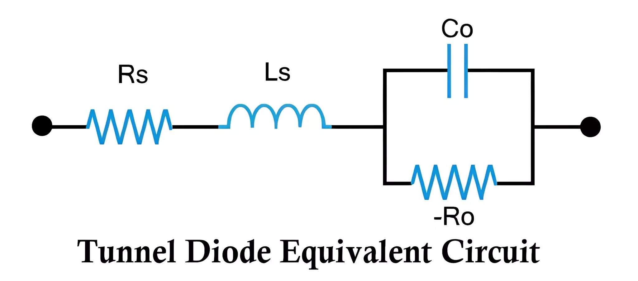
- -Ro = Negative resistance
- Co = Junction capacitance
- Rs = Series resistance
- Ls = Series inductance
Operation & Frequency Response
- Low Frequencies: The inductor Ls can be ignored, and the circuit behaves mainly as a parallel RC network with negative resistance.
- High Frequencies: The inductance Ls becomes significant, affecting oscillations and stability.
- Oscillation Condition: When the negative resistance -Ro cancels out the losses from Rs, the circuit can sustain oscillations, making tunnel diodes useful in high-frequency oscillators.
Advantages of Tunnel Diode
- High-Speed Operation: The tunneling effect allows the tunnel diode to operate at very high frequencies, making it suitable for microwave and RF applications.
- Low Power Consumption: The tunnel diode requires very low power to operate, making it energy-efficient.
- Compact Size: Tunnel diodes are small in size, making them suitable for integration into compact electronic devices.
- High Switching Speed: The tunneling mechanism allows for extremely fast switching, making the tunnel diode ideal for high-speed digital circuits.
- Negative Resistance: The negative resistance region can be exploited in oscillator and amplifier circuits to achieve high-frequency operation.
Disadvantages of Tunnel Diode
- Low Peak-to-Valley Current Ratio: The ratio of the peak current Ip to the valley current Iv is relatively low, limiting the efficiency of some applications.
- Temperature Sensitivity: The performance of tunnel diodes is highly sensitive to temperature variations, which can affect their stability and reliability.
- Low Output Power: Tunnel diodes typically have low output power, making them unsuitable for high-power applications.
- Complex Fabrication: The heavy doping required for tunnel diodes makes their fabrication process more complex and costly compared to conventional diodes.
- Limited Applications: Its unique characteristics limit tunnel diodes to specific high-frequency applications, making them less versatile than other types of diodes.
Applications of Tunnel Diode
Despite their limitations, tunnel diodes have found use in several specialized applications, particularly in high-frequency circuits. Some of the key applications include:
- Microwave Oscillators: The negative resistance region of the tunnel diode makes it ideal for use in microwave oscillators, where it can generate high-frequency signals.
- High-Speed Switching Circuits: The fast switching speed of tunnel diodes makes them suitable for use in high-speed digital circuits, such as frequency counters and pulse generators.
- Amplifiers: Engineers use tunnel diodes in low-noise amplifiers, especially in microwave and RF applications, to exploit their negative resistance for gain.
- Frequency Converters: Designers integrate tunnel diodes into frequency converters to mix two input signals and generate an output signal at a different frequency.
- Relaxation Oscillators: Circuit designers utilize the tunnel diode’s negative resistance region to build relaxation oscillators for timing circuits and signal generation.
- Memory Storage: Researchers explore tunnel diodes for memory storage devices, particularly in quantum computing and other advanced technologies.
- Sensors: The sensitivity of tunnel diodes to external conditions, such as temperature and radiation, makes them suitable for use in various sensing applications.
Conclusion
The tunnel diode is a unique semiconductor device that leverages the quantum mechanical tunneling effect to achieve high-speed operation and negative resistance. Its construction involves heavily doped P-type and N-type materials, resulting in a narrow depletion region that facilitates tunneling. The I-V characteristics of the tunnel diode are distinct, featuring a negative resistance region that makes it valuable in high-frequency applications such as microwave oscillators, amplifiers, and high-speed switching circuits.
While the tunnel diode offers several advantages, including high-speed operation and low power consumption, it also has limitations such as temperature sensitivity and low output power. Despite these drawbacks, specialized applications continue to utilize the tunnel diode for its unique properties.
As technology continues to advance, the tunnel diode may see further innovations and applications, particularly in the fields of quantum computing and high-frequency electronics. Understanding the principles, characteristics, and applications of the tunnel diode is essential for engineers and researchers working in these cutting-edge areas. You can see the datasheet of 1N3716 tunnel diode.
Types of Diodes with Symbol, Definition, Working and Applications
