MOSFET Full Form is Metal Oxide Semiconductor Field Effect Transistor. Here we will be discussing MOSFET VI Characteristics, symbol and its classification. They are broadly classified into two types namely enhancement Type and depletion type MOSFET.
In an enhancement type MOSFET channel has to be induced for the device to conduct, which is achieved by increasing Vgs voltage above the threshold voltage.
Since increase in Vgs voltage enhances the channel, hence it is called an enhancement type MOSFET. Another type of MOSFET is the depletion type in which the channel exists even when it is unbiased. Each is further classified either as an n-channel MOSFET or a P-channel.
A threshold voltage is required for channel formation in enhancement type MOSFET. Vt is always positive for n-channel MOSFET we expect to apply a positive voltage to the gate terminal to induce the channel.
Thus a positive value for Vt means the applied voltage must be larger than this threshold voltage to obtain strong inversion and a conducting n-channel.
Enhancement type MOSFETs are of two kinds:
- N-channel enhancement type MOSFET
- P-channel enhancement type MOSFET
N-type MOSFET Symbol:
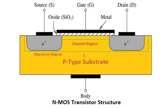
The physical structure of n-channel enhancement type MOSFET Starting material for nMOS fabrication is a p-type substrate.
The source and drain are heavily doped
formed by diffusing n-type impurities through a suitable mask into these areas.
Thus, source and drain are isolated from one another by two diodes. A thin layer of silicon dioxide is grown on the surface of the substrate, covering the area between the source and the drain regions.
Gate electrode of the device is formed by depositing metal on the top of the oxide layer. Metal contacts are taken out from the source region, drain region, and the body. Hence, MOSFET is a four-terminal device named gate, source, drain, and the body terminal.
A conducting channel will eventually be formed
through applied gate voltage in the section of the
device between the drain and the source diffusion regions.
The distance between the train and the source diffusion region is the channel length L, find the lateral extent of the channel is the channel width.
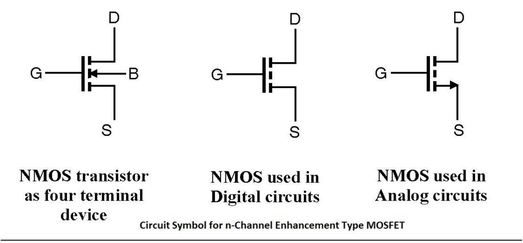
N-type MOSFET Symbol:
The figure shows a circuit symbol of an nMOS transistor. The first symbol is the four-terminal symbol while the latter shows the MOSFET symbol with source, drain and gate shorted giving a three-terminal symbol of the nMOS transistor.
MOSFETs name is derived from its physical structure. The name however has become a general one and is used also for the FETs that do not use metal for the gate electrode.
In fact, metal is mostly supplanted by heavily doped polycrystalline silicon at the microscopic level consists of small regions of silicon crystal called crystallites.
The term polycrystalline arises from viewing the material as being made up of randomly distributed crystallites. It has the same melting temperature as crystal silicon.
This allows the wafer to be subjected to the processing steps that require high heat treatment after the gate has been formed making it much suitable material than metal.
Also, polycrystalline silicon can be doped to any level. For example during ion implantation for the formation of source and drain regions polysilicon also gets doped.
Another name for MOSFET is the insulated gate FET or IGFET however, this label is not used commonly. It is named so, from its Structure where the gate electrode is electrically insulated from the device body.
pMOS Transistor:
The p-channel pMOS uses n-type semiconductor material as a substrate with p+ regions for the source and drain regions.
The device operates in the same manner as an n-channel device. holes as the charge carriers that is, wherever there was n-type silicon in the nMOS transistor are now p-type silicon in pMOS transistor, and similarly wherever there was p-type si is now n-type is in the pMOS transistor.
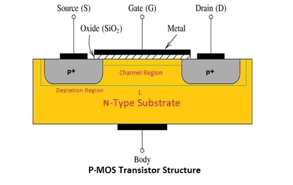
Therefore, to form an inversion layer beneath the gate, we need to attract holes to the gate electrode, Thus, Vgs voltage must be sufficiently negative. The threshold voltage (Vt) is hence a negative value.
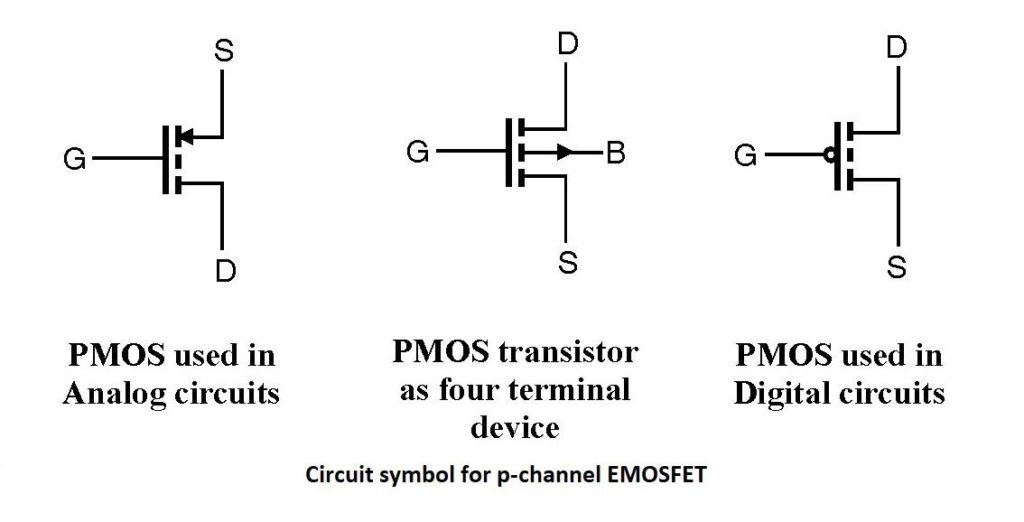
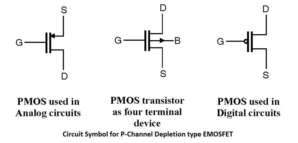
Also, for current to flow through the channel Vds voltage applied must be negative. Therefore Vgs, Vds, and Vt are negative for the pMOS transistor. Also, the current direction is from the source to the drain terminal. Shows the circuit symbol for the p-channel enhancement type MOSFET.
MOSFET VI Characteristics Id vs Vds Graph:
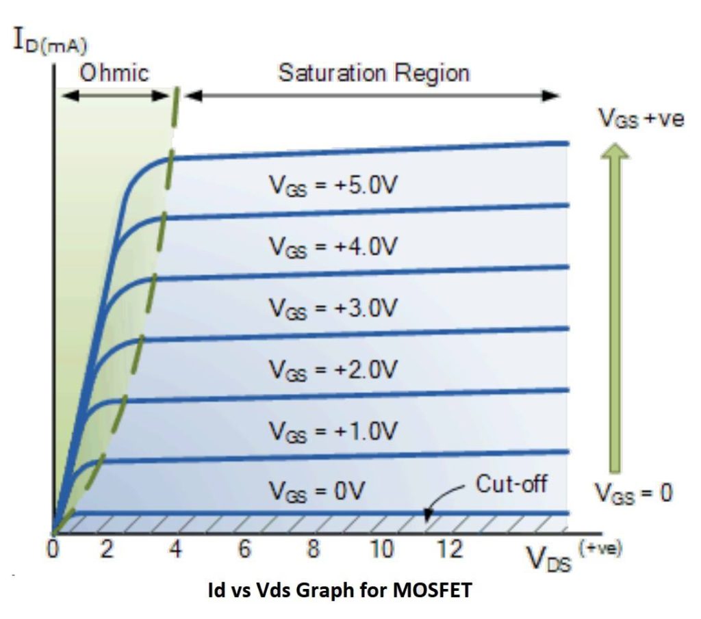
From the above MOSFET VI characteristics, you can see that a has three regions of operation, namely cut-off, saturation, and ohmic region. In the cut-off region, it is in an OFF state whereas in the saturation region it acts as an amplifiere, and in the ohmic region, it behaves as an open switch.
In the above graph, you can see that as we increase the Vds voltage the current Ids first increases, and then it becomes almost constant.
MOSFET VI Characteristics Id vs Vgs graph:
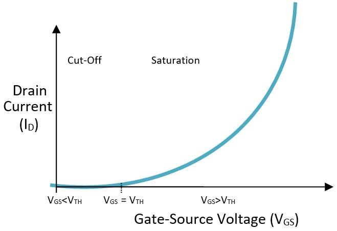
The drain current increases exponentially as the Vgs voltage increases and then becomes constant. As shown in the MOSFET VI characteristics there is a minimum gate to source voltage known as threshold voltage at which current just starts flowing through the channel.
Advantages of nMOSFET over pMOSFET:
Now a day’s, n-channel MOSFETs have become much popular and are used extensively for fabricating MOS circuits and systems than p-channel MOSFETs. The P-channel MOSFETs find their use only in Complementary Metal Oxide Semiconductor (CMOS) integrated circuits.
The main advantage of n-channel MOS transistor over p-channel MOSFET is due to the fact that the charge carries in n-channel devices are the electrons, which have the mobility of about 1300 cm²/Vs.
On the other hand, the charge curries in. p-channel devices are the holes that have the mobility of about 500 cm²/Vs.
Since the current in a semiconductor is directly proportional to the mobility, therefore the current in n-channel MOSFETs is more than two to three times that of p-channel MOSFETs for the same dimensions. The ON resistance of the n-channel MOSFETs is one-third of that for p-channel MOSFETs.
It means that in order to achieve the same value of current and ON resistances, the p-channel MOSFET requires three times the area of an equivalent n-channel MOSFET.
Thus, electronic circuits using n-channel MOSFETs are much smaller in size than those of p-channel MOSFETs. This result is in higher packing density.
Depletion Type MOSFET:
There are two types of depletion type MOSFETs
- n-channel depletion type MOSFET
- p-channel depletion type MOSFET
Although depletion type MOS transistor is to some extent similar in construction and in operational modes to that of enhancement type MOSFETs but has one important distinction.
The depletion type MOSFET inherently has a channel.
Even when the gate terminal is not biased, it has an n-type region connecting the n+ source and the drain regions (for n-channel depletion type MOSFET) at the surface of the semiconductor even when the gate terminal is not biased.
Thus if a voltage Vds is applied between drain and source, a current Id flows for Vgs = 0, So, unlike enhancement MOSFETs, there is no need to induce a channel in depletion type MOSFET.
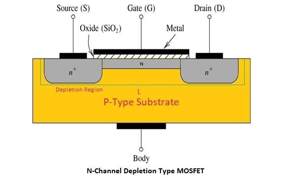
Shows the circuit symbol for the n-channel depletion type MOSFET.
n-Channel Depletion Type MOSFET
It consists of a p-type silicon substrate formed from silicon semiconductor, This substrate acts as a supporting body over which the device is constructed.
N-type material is diffused into the substrate to form the drain and the source. An n-channel region is present that links the source and drain regions together as shown.
The transistor has four terminal gate, drain, source, and body. Three terminals are shown in the diagram. As we have seen the gate, and the substrate are isolated from each other due to the Presence of silicon dioxide between them.
Silicon dioxide being an insulating material provides no electrical connection between the gate terminal and the channel of the MOSFET, this gives rise to a very high input impedance of the device and the gate current is almost zero.
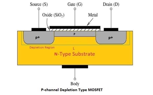
p-Channel Depletion Type MOSFET:
The construction of a p-channel depletion type MOSFET is similar to that of n-channel MOSFET but with an n-type substrate and p-type of source and drain regions. Hence, the voltage polarities and the current directions for a P-MOSFET are reversed.
p-channel depletion type MOSFETs contain a channel (even when unbiased) consisting of holes.
What is Scaling of MOSFET, Scaling Factor, and Types of Scaling


Great article. Do more about these subjects. It’s very cool.
Thank You