In this article you will see how to make 4-bit adder in Verilog.

Table of contents
1 What is a 4-bit adder?
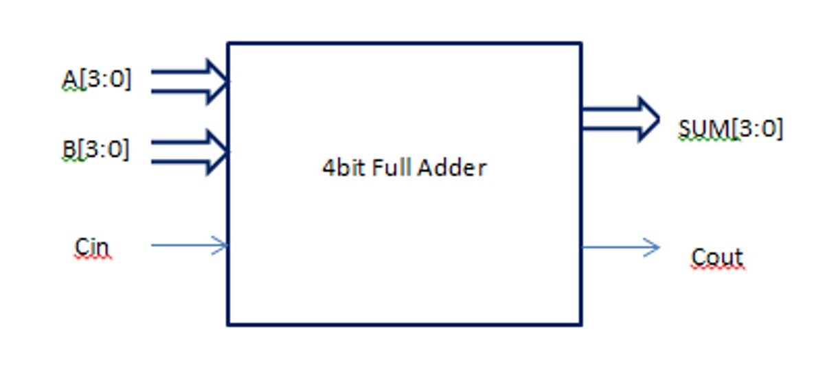
2 4-bit adder Schematic
3 Video related to 4-bit adder Verilog
4 Verilog Full Adder
5 Truth Table of full adder
6 Design of full adder
7 Full adder schematics
8 4-bit adder Verilog Code
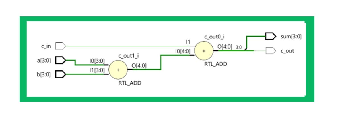
9 RTL Schematic
10 RTL Verilog
A digital circuit known as a “4-bit adder” produces a 4-bit total from two four-bit inputs. At the output, a 1 bit carry is produced. The Full Adder was used to create a 4 bit adder in the code below. In the main module, the Full adder has been instantiated four times. The Full Adder requires ‘a’ and ‘b’ as its first two inputs, and ‘cin’ as its third. The Full Adder’s equations are as follows:
module Multi-bit Adder(a,b,cin,sum,cout);

input [3:0] a,b;

input cin;

output [3:0]sum;

output cout;

assign {cout,sum}=a+b+cin;

End module
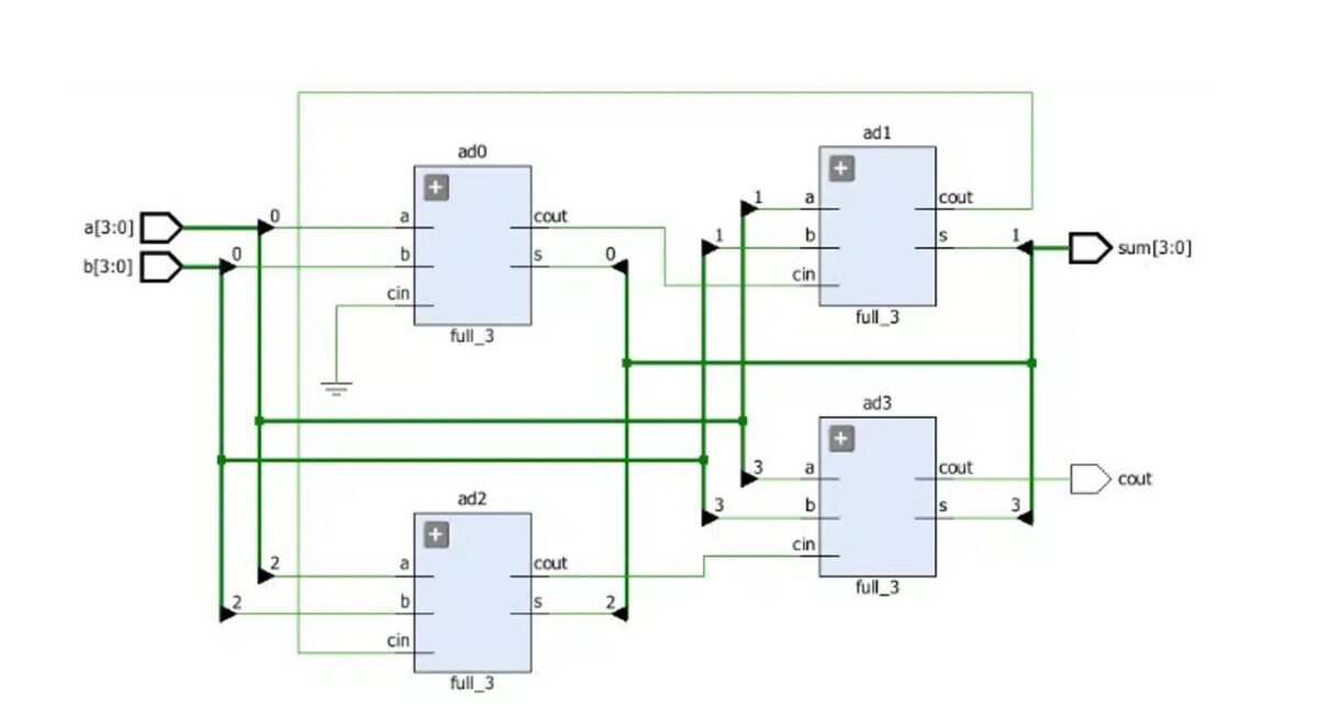
4-bit adder schematic:
Video related to 4-bit adder in Verilog
Verilog Full Adder:
A digital component known as an adder adds two numbers together. It is used to increase addresses, table indices, buffer pointers, and many other locations where addition is necessary. It is the primary component inside an ALU of a processor. A complete adder generates a total and a carry output by adding a carry input and additional binary values.
Using logic gates, the full adder is a digital component that executes three numbers. It is the primary element of a processor’s ALU and is used to increase addresses, table indexes, buffer pointers, and other locations where addition is necessary. A one-bit complete adder produces a total and a carry bit after adding three one-bit binary values, two input bits, and one carry bit.
By employing two half adders and ORing their outputs, a full adder is created. Two binary numbers are added via a half adder. The full adder is a combinational circuit, allowing for Verilog modeling. Below is the logical expression for the two outputs, sum and carry. For two-bit binary values, the input variables are A and B, the carry input is Cin, and the output variables for Sum and Carry are Cout.
Truth Table of full adder
19″>
00000
| 0 | 0 | 1 | 0 | 1 |
| 0 | 1 | 0 | 0 | 1 |
| 0 | 1 | 1 | 1 | 0 |
| 1 | 0 | 0 | 0 | 1 |
| 1 | 0 | 1 | 1 | 0 |
| 1 | 1 | 0 | 1 | 0 |
| 1 | 1 | 1 | 1 | 1 |
Design of full adder
The 4-bit signals a and b are used to input two binary numbers into a 4-bit adder, which is an example of one. An adder can be expressed in Verilog using a continuous assignment with assign or an always block with a sensitivity list that includes all inputs because it is a combinational circuit. The code for the earlier method is displayed below.
An always block is used in the code below, and it is activated whenever any of its inputs change value.
module fulladd  input [3:e] a

input [3:e] b

input c_in,

output reg c_out,

output reg [3:@] sum);

always @(a or b or cin) begin

(c_out, sum] = a + b + c in;end

End

Module
Full adder schematic
Code for a 4-bit adder in Verilog:
The following is the Verilog code for the 4 Bit Adder using a Full Adder:
Test Bench:
You can use simulation to check if your FPGA or ASIC design performs as expected by taking a closer look at it. Virtex-7 FPGAs, Kintex-7 FPGAs, and other FPGA series all can use simulation to check their situation. The stimulus for the simulation is provided by a testbench.
Each combination of chosen lines is tested on the test bench to ensure that the proper input and output are connected. The following is the test bench code in Verilog for the 4 Bit Adder using the Full Adder:
module TestModule;

// Inputs

reg [3:0] a;

reg [3:0] b;

reg cin;

// Outputs

wire [3:0] sum;

wire cout;

// Instantiate the Unit Under Test (UUT)

MultibitAdder uut (

.a(a),

.b(b),

.cin(cin),

.sum(sum),

.cout(cout)

);

initial begin

// Initialize Inputs

a = 0;

b = 0;

cin = 0;

// Wait 100 ns for global reset to finish

#100;

a = 2;

b = 3;

cin = 1;

// Wait 100 ns for global reset to finish

#100

end

endmodule
RTL Schematic:

RTL Verilog:
Register transfer level is referred to as RTL. This suggests that the Verilog code you wrote defines how data is altered as it is transferred between registers. The combinational logic that sits between the registers transforms the data on the fly.
Two components make up a synchronous circuit, such as:
Sequential logic registers: The only components in the circuit with memory qualities are registers, which synchronize circuit action to clock signal edges. And D flip-flops are typically used to implement them.
Combinational logic:
Combinational logic executes each of the circuit’s logical operations. Additionally, logic gates are present.