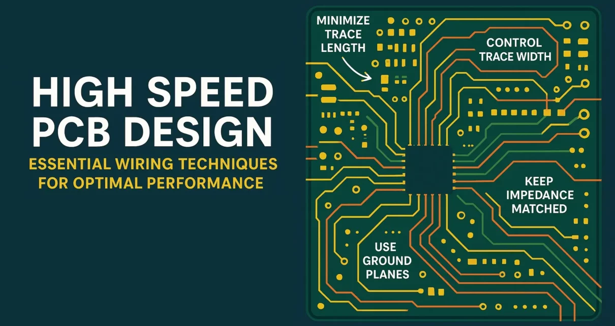
In modern electronics, high speed PCB design is critical for ensuring signal integrity, reducing EMI, and maximizing performance. Whether you’re designing for IoT, 5G, or high-frequency applications, mastering PCB design and layout techniques is essential. Below, we break down advanced high-speed PCB design techniques, including signal routing, impedance control, and thermal management, while highlighting how professional PCB design and layout services can streamline development.
1. Signal Routing for High-Speed PCB Design
Microstrip vs. Stripline in High-Speed Layouts
- Microstrip (surface traces over a ground plane) is common in high-speed PCB design due to its simplicity, but it’s more susceptible to EMI.
- Stripline (traces embedded between two ground planes) offers superior noise immunity, making it ideal for high-frequency PCB layouts.
Example: In 10Gbps+ designs (e.g., PCIe, DDR5), stripline routing minimizes crosstalk and maintains consistent impedance.
Differential Pair Routing Techniques
- High-speed differential signals (USB 3.2, HDMI, Ethernet) require tight length matching (±5 mil tolerance) and controlled spacing to prevent skew.
- Use 3W rule (spacing = 3x trace width) to reduce crosstalk in dense PCB layouts.
General High-Speed Routing Best Practices
- Minimize vias (each via adds ~0.5–1nH inductance).
- Avoid 90° bends (use 45° or arcs) to prevent impedance discontinuities.
- Route critical signals first (clocks, RF lines) before general traces.
2. Power & Ground Design for Noise Reduction
Power Integrity in High-Speed PCBs
- Use wide power traces (e.g., 50 mils for 5A current) or power planes to minimize IR drop.
- Implement decoupling capacitors (0.1µF near ICs + bulk 10µF) for stable voltage.
Advanced Grounding Techniques
- Split ground planes (analog/digital/RF) with a single-point star connection.
- Multi-layer PCBs should dedicate entire layers to ground for low impedance return paths.
Pro Tip: Professional PCB design and layout services use 3D EM simulation tools (e.g., Ansys HFSS) to optimize power delivery networks (PDNs).
3. Impedance Control & Signal Integrity
Controlled Impedance Routing
- Calculate trace impedance using Polar SI9000 or AltStack (factors: dielectric constant, trace width, layer spacing).
- High-speed signals (e.g., USB4, Thunderbolt) often require 50Ω (single-ended) or 100Ω (differential) impedance.
Mitigating Signal Loss in High-Frequency PCBs
- Low-loss laminates (Rogers, Isola) for >5GHz designs.
- Via stitching around high-speed traces to reduce ground return loops.
4. Thermal Management in High-Power PCB Layouts
Heat Dissipation Strategies
- Thermal vias under hot components (e.g., FPGAs, power MOSFETs).
- Copper pours + exposed pads for passive cooling.
Thermal Simulation in PCB Design Services
Advanced PCB design and layout services leverage CFD analysis (e.g., FloTHERM) to predict hotspots and optimize airflow.
Circuit Designing Guidelines, Key Rules and Best Practices
The Value of Professional PCB Design Services
For mission-critical high speed PCB design, partnering with an experienced PCB design service like FanyPCB delivers measurable advantages:
Signal Integrity Validation – Using industry-standard tools like HyperLynx and Sigrity, FanyPCB design service ensures optimal performance for even the most complex PCB design projects.
DFM/DFT Compliance – Their expertise minimizes manufacturing risks, helping you avoid costly defects and production delays in your PCB layout and fabrication process.
Fast-Track Prototyping – Many professional services, including FanyPCB, offer accelerated PCB design and prototyping, with some providing 24-hour turnaround for time-sensitive projects.
Whether you’re developing high-frequency boards or complex multilayer systems, leveraging a specialized PCB design service ensures reliability, efficiency, and manufacturability.
Gold Finger PCB Assembly: Best Practices for Ensuring Reliability
