How does the 555 Timer work? NE555 is one of the most popular and widely used ICs of all time. In this blog, we will discuss the working of the 555 timer IC.
Overview
The 555 Timer was designed by Hans Camenzind in 1971. It can be found in vast variety of electronic devices. 555 timer is used to produce time delay and a square wave of a wide range of frequencies. It is highly accurate and stable. The 555 Timer has three astable, monostable, and bistable mode.
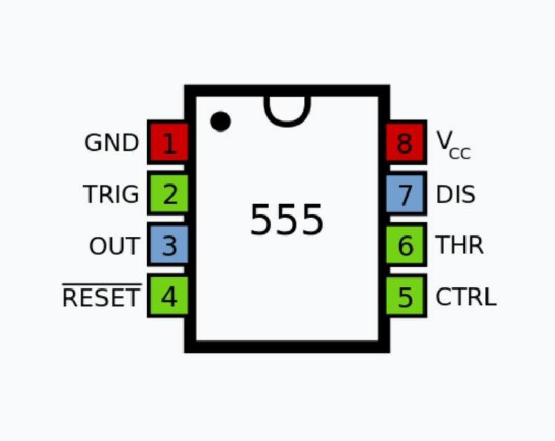
To understand the working of 555 timer let’s take a look inside this IC.
You can download the datasheet of 555 timer from here
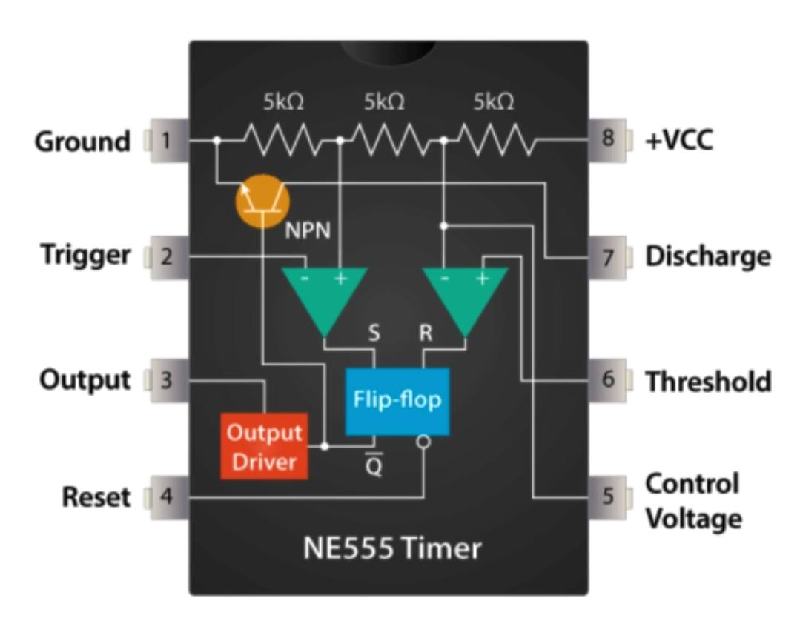
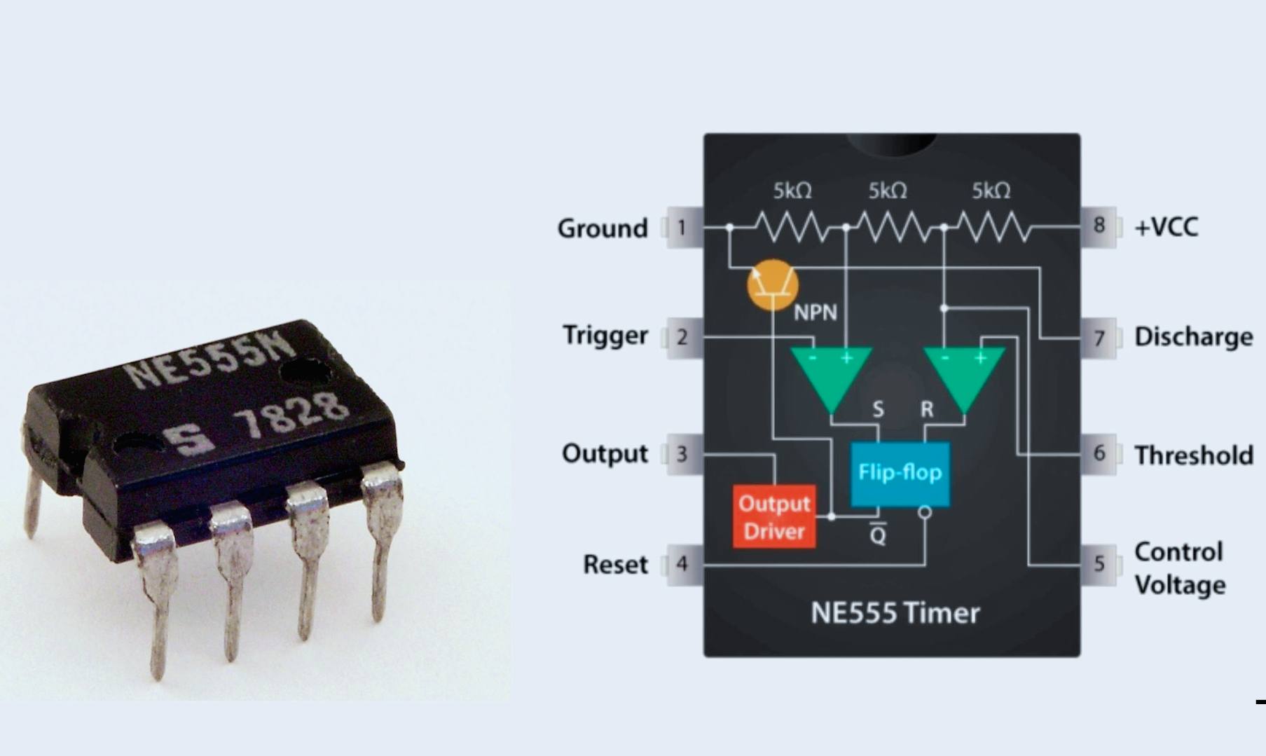
The internal structure of the 555 Timer IC
555 Timer consists of 25 transistors, 2 diodes, and 15 resistors.
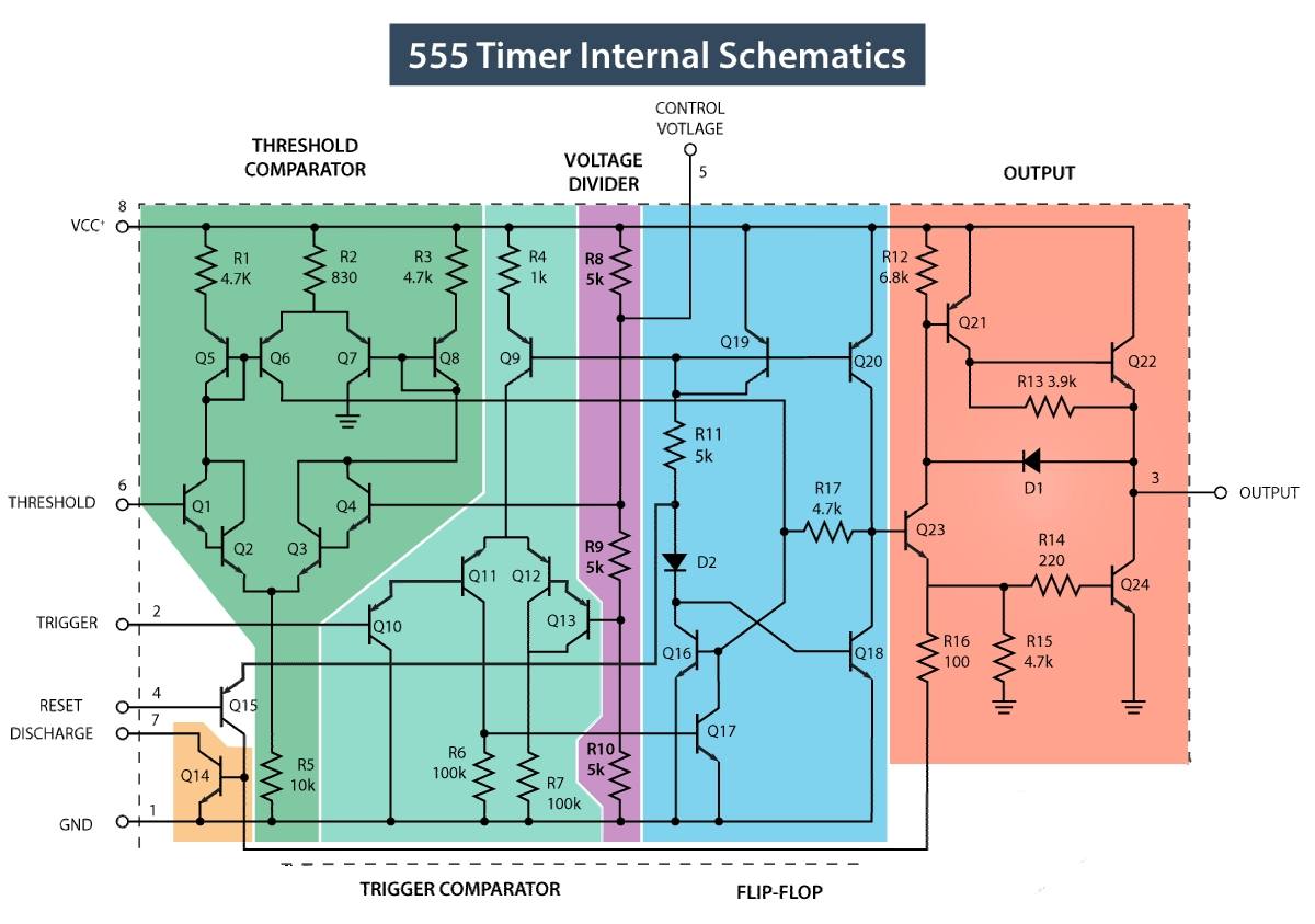
Its block diagram consists of 2 comparators, one flip-flop, a voltage divider, a discharge transistor, and an output stage.
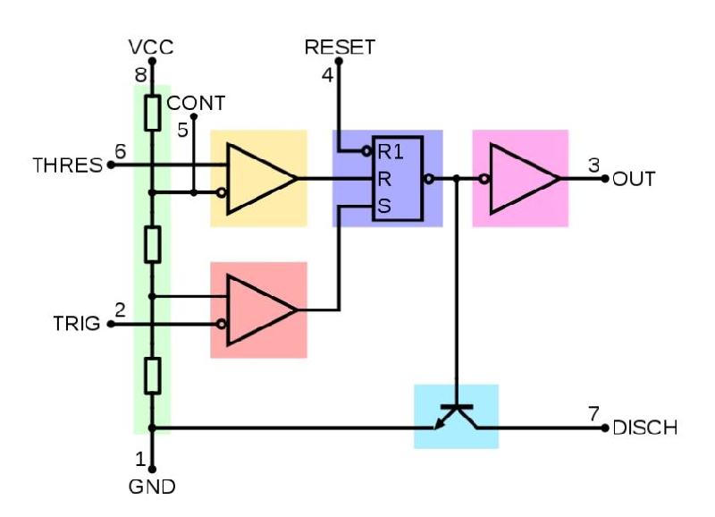
The voltage divider consists of three similar 5k resistors which makes two reference voltages at 1/3 and 2/3 of input voltage ranging from 5 to 15V.
In the next stage, there are two comparators. It compares two analog input voltages at its positive (non-inverting) and negative (inverting) input terminal. If the input voltage at the positive terminal is higher than the input voltage at the negative terminal it will give 1(High) output. If the voltage at the negative terminal is higher than the voltage at the positive terminal, the comparator output will be 0(low).
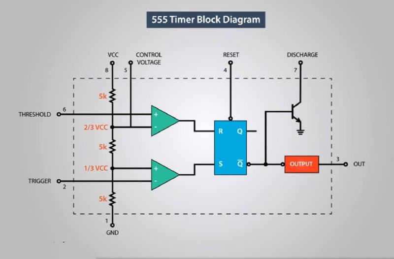
The negative input terminal of 1st comparator is connected to the 2/3 reference voltage and external “control” pin, where’s the positive input terminal to the external “Threshold” pin.
The negative input terminal of the second comparator is connected to the “Trigger” pin and the positive input terminal to the 1/3 of the voltage divider.
By using these three pins( Trigger, Threshold, and Control) output of the two comparators is controlled which are then fed to the R and S inputs of the flip-flop next stage flip-flop.
The flip-flop will output 1 when R is 0 and S is 1 and output will be 0 when R is 1 and S is 0. Also, the flip-flop can be reset by the external pin number 4 called reset.
The Q-bar output of the flip-flip goes to the output stage. The output of the flip-flip is also connected to a transistor that connects the “Discharge” pin to the ground.
Working of 555 timers in Astable Mode:
In astable mode 555 IC becomes an oscillator or a Free Running Multivibrator. It continuously switches between High and Low without applying any external trigger.
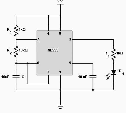
We need two resistors and a capacitor. The Trigger and Threshold pins are connected together. Initially, the voltage source will start charges the capacitor through the Resistors R1 and R2.
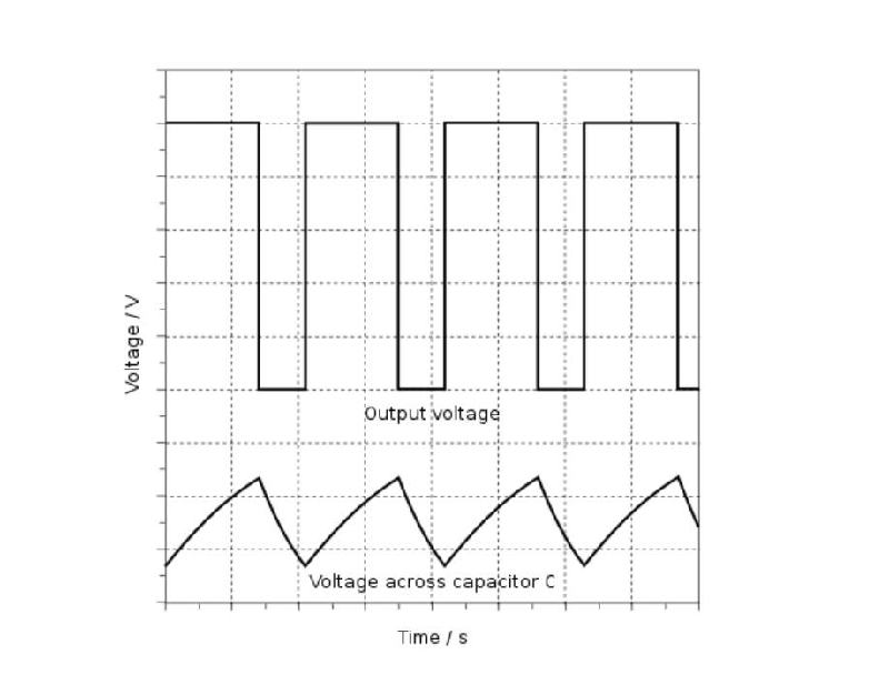
The input voltage at the Trigger pin is still lower than 1/3 of the supplied voltage due to this the Trigger comparator will output 1. This makes Q-bar output 0 and the discharge transistor is closed. At this time the 555 Timer output is High.
Once the voltage of capacitors reaches 1/3of of the voltage divider The comparator output goes to 0(low). The flip-flops output remains zero. When the voltage at the capacitor reaches 2/3of the voltage divider output of the Threshold comparator becomes 1 which makes flip-flop output 1(High).
When the flip-flop output becomes 1 it makes discharge Transistor active which then starts discharging the capacitor through R2. During this time the output of 555 timers is 0(low).
While discharging the voltage across the capacitor starts to decline, and the Threshold comparator gives output 0. which doesn’t make a change since both R and S inputs of the flip-flop are 0.
But once the voltage across the capacitor drops to 1/3 of the supplied voltage the output of the trigger comparator becomes 1. Due to this discharge transistor turns off and the capacitor will start charging again. This process of charging and discharging between 2/3 and 1/3 of the input voltage will keep working automatically due to this square wave is produced at output of 555 Timer.
We can calculate the time and frequency of the output. The off-time and ON-time give time of one cycle of a square wave.
If we modify this circuit and change the R2 resistor by a variable resistor or a Potentiometer, we can control the frequency and the duty cycles of the square wave. We can make a PWM DC motor speed controller using the 555 Timer using this mode of operation.
Working of 555 timer in Monostable mode
In monostable mode, the output of 555 timer is a pulse which ends when the voltage at the capacitor becomes 2⁄3 of the supply voltage. The output pulse width can be increased or decreased by adjusting the values of R and C.
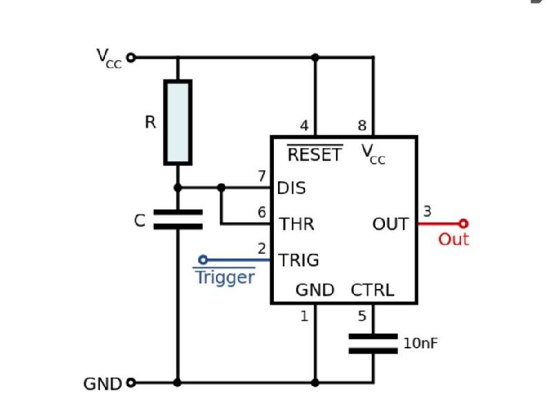
To understand it’s working Assume initially the output of the monostable is zero. the output of the flip-flop is 1 so that the discharging transistor is on and the voltage across a capacitor is zero. The negative input of upper comparator is at 2/3 of supply voltage and the other is connected to a capacitor. For lower comparator, one input is trigger pulse and positive input is connected at 1/3 of supply voltage.
Now the capacitor charges toward supply voltage(Vcc). When the trigger input is a high voltage the output of the lower comparator is 0 meanwhile upper comparator is also 0. Hence the output of flip-flop remains 0( unchanged). when the voltage across capacitor crosses the 1/3 of the Vcc the output of lower comparator goes from 0 to 1. The flip-flops output becomes 0 and output of monostable mode is high. The discharging transistor is still off and capacitor charges towards Vcc from 1/3 of Vcc.
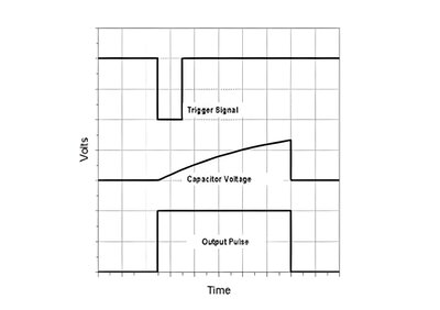
When the voltage across capacitor crosses 2/3 of VCC, the upper comparator changes from 0 to 1 which makes flip flops output 1, and the output of monostable is 0. The discharging transistor becomes on and the capacitor discharges through this transistor due to a low resistance path. The cycle repeats continuously if again trigger input is applied. The charging and discharging of the capacitor depend on the RC time constant.
The voltage across capacitor is given by VC = VCC(1-e^(-t/RC))
555 timer in Bistable mode
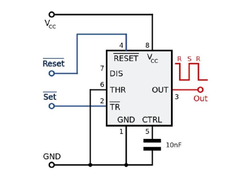
In bistable mode, the 555 timer acts as an SR flip-flop. The trigger and reset inputs (pins 2 and 4 ) are kept high via pull-up resistors. The threshold input (pin 6) is grounded. In this configuration when trigger input is connected to ground acts as a ‘set’ making output high. Keeping the reset input to ground acts as a ‘reset’ making output low. Set causes a rising edge and reset causes falling edge. No timing capacitors are required in a bistable configuration.
Universal NOR Gate Truth Table, Logic Circuit and IC PIN Diagram

One Reply to “Working of 555 Timer IC Explained”