What are flip flops in electronics? A flip-flop is an electronic circuit that can store single-bit binary data either logic 0 or logic 1. Basically, a flip flop is a Bistable multivibrator that changes its output depending on the input. Flip Flops are of two types edge triggered, and level triggered. State of an Edge triggered flip flop changes during the positive or negative edge of a clock cycle. Whereas in the case of level-triggered flip flop output can change during high or low clock duration. Level triggered flip flops are called latch, they are transparent because when they are enabled their output becomes the same as the input.
What is the difference between a flip flop and a latch?
The main basic difference between a flip flop and a latch is the clock triggering mechanism.
A Flip Flop is an edge-triggered device whereas a latch is a level-triggered device.
Latches come under combinational circuits whereas flip flops come under sequential circuits.
Combinational circuit:
In a combinational circuit, the output depends only on the present input. Its speed is fast and easy to design as compared to the sequential circuit. It is used for Arithmetic and Boolean operation.
Sequential circuit:
In the case of the sequential circuit, output depends on present input as well as past input. Its speed is slow and it is difficult to design as compared to the combinational circuit. But the main advantage of a sequential circuit is that it has a memory so it can store information.
Let’s see how a Latch made from NAND gates works:
We will start with a very basic SR latch. As you can see it is composed of two NAND gates having two inputs. The first NAND gate has an S bar as input and the second one has an R bar as input. The output of both the NAND gates is connected to the input of the other NAND gates. The output of the first NAND gate is Q whereas the output of the other gate is the Q bar. If one output is at logic low then the other one will be at logic high.
This is an active-low circuit when we apply low logic to set pin output at Q goes to logic 1 and Q bar becomes logic 0. When we apply logic low to reset pin output at Q becomes logic low and Q bar goes to logic 1. This is how SR latch works, its output is dependent on present input, and it cannot store data.
Types of Flip Flop in Digital Circuit:
Now we will see four major types of flip flop SR flip flop, JK flip flop, D flip flop, and T flip flop.
SR Flip Flop:
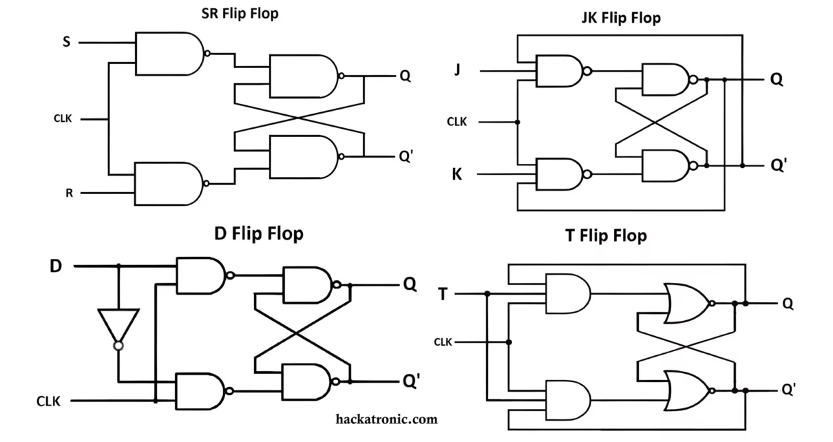
In SR flip flop we connect NAND gates at the inputs of SR latch and also a clock signal is given to inputs of NAND gates to make it asynchronous sequential circuits. Now Set and Reset pins have become active High signals and remaining things are the same.
See the truth table for SR Flip Flop:
JK Flip-Flop:
from the truth table, you can see that when the set pin is high output Q is high, and when the reset pin is high Q’ is high. But here is a problem that when both the inputs are at logic 1 output goes to an undefined state.
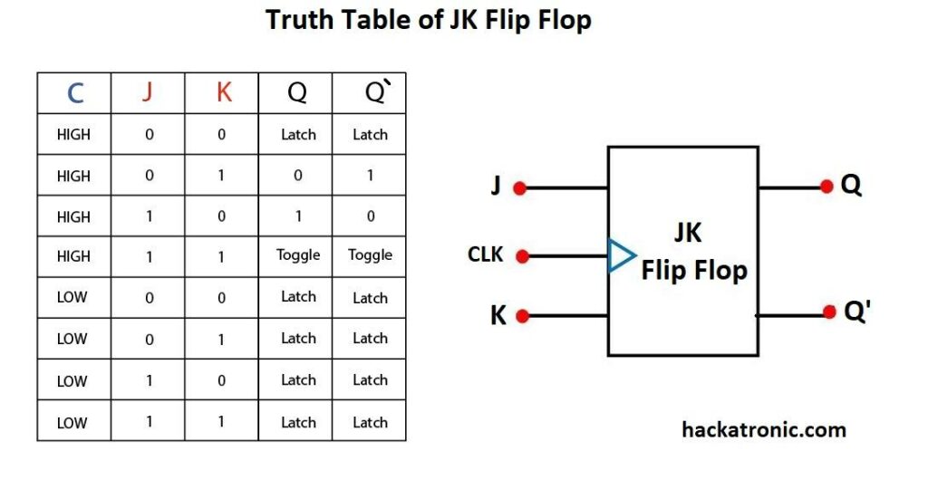
JK flip flop is an improved version of SR flip flop. The problem of the undefined state in the SR flip flop is solved in the JK flip flop. To solve this problem in SR flip flop we require another flip flop. In the JK flip flop if J=K=1 occurs then output gets toggled with respect to the previous output.
In the JK flip flop, we use a three-input NAND gate, and output from one side is given as input to the NAND gate on the opposite side. This is an active-high input circuit.
See the truth table of JK flip flop:

T(Toggle) Flip Flop:
From the truth table, you can see that when the output at both J and K inputs is different output Q follows the value of J during the next clock edge. If both J and K are at logic Low no changes occur at the output. When both J and K are at logic High the output gets toggled from one state to another state.
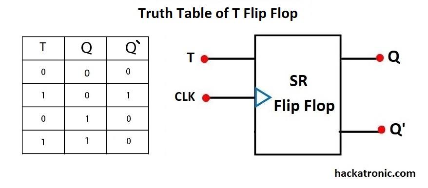
A T flip flop is actually a JK flip flop, the only change is that both the input are given the same logic and a clock signal is given. The output of the T flip flop remains unchanged when both the inputs are the same. When both the inputs are different output gets toggled or complemented hence name T flip flop.
See the Truth Table of T Flip Flop:

D(Data) Flip Flop:
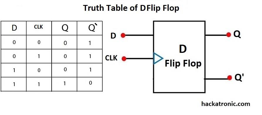
D flip flops are very popular in Digital Electronics, they are widely used in counter circuits, shift registers, and synchronization circuits. In this flip flop, there is a not gate present between inputs of JK flip flop, and the clock signal is given. In this flip flop output changes only during the edge of the clock signal.
See Truth table of D flip flop:

Applications of Flip Flop in Electronics:
From the truth table, you can see that the output changes only when input and clock both are high and it changes at the edge of the clock cycle.
Flip Flops are the basic building blocks of many Digital electronics circuits. Here are some applications of flip flops.
- Counters.
- Shift Registers.
- Storage Registers.
- Frequency Dividers.
- Data transfer.
- Data storage.
- Bounce elimination switch.
- Memory
- Latch.
- Registers


