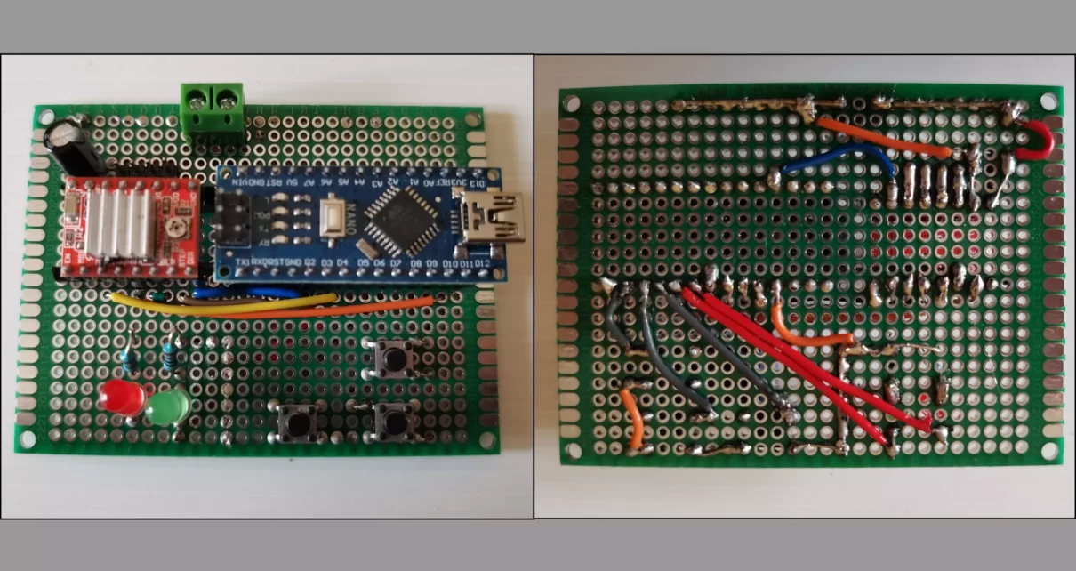
The word “proto” refers to the essential initial stage of electronic invention. An electronic circuit design’s physical form is represented by a prototype circuit board or proto-circuit board. Engineers can test and improve their ideas with this first construction, transforming abstract thoughts into practical realities.
Consider a proto HDI PCB to be the prelude to the big opening night. Just like performers refine their performance on stage in front of an audience, engineers use them to find and fix any design defects or performance concerns prior to mass manufacturing. This important stage guarantees that the finished product fulfills industry standards, performs as planned, and offers a flawless user experience.
This thorough blog post on proto-circuit boards describes the various fabrication methods and their importance to the electronics development cycle. We’ll assist you in choosing the best proto-circuit board for your particular needs.
Prototype Circuit Board History:
Electronics prototyping has a rich and interesting past. Over time, the procedure changed in tandem with improvements in technology. When engineers first started out, they used simple tools like wire wrapping and breadboards to build prototypes. These techniques were laborious, prone to mistakes, and simplistic.
Prototyping was forever changed with the introduction of printed circuit boards (PCBs). PCBs provided a more dependable and small solution, allowing engineers to design more intricate circuits with higher accuracy. However, the rather long and expensive initial PCB production process hampered rapid prototyping.
The introduction of proto-board PCBs made specifically for prototyping was another important turning point. These boards were perfect for iterative design and testing because of their shorter lead times and reduced prices.
With improvements in manufacturing processes, materials, and design tools, proto-board PCBs have continued to evolve. This has sped up the development process and allowed engineers to commercialize their ideas more quickly than in the past.
The electronics industry has been greatly impacted by prototype printed circuit boards. They have made it possible for engineers to thoroughly test their designs, investigate novel concepts, and drastically shorten time-to-market. Proto-board PCBs have been instrumental in developing the current electronics industry, from consumer electronics to medical devices and aerospace technologies. In the upcoming years, their ongoing evolution should spur even more innovation and advancement.
Parts of a Working Circuit Board:
A proto-circuit board is an intricate assembly of components working together to form the foundation of electronic prototypes. Understanding its core elements is essential to appreciating the role of proto-board PCBs in the development process.
The substrate material acts as the board’s base, providing structural support for all components. Common substrate materials include phenolic paper, FR-4 (a flame-retardant fiberglass epoxy laminate), and flexible polyimide. The choice of substrate depends on factors such as the circuit’s intended application, mechanical strength, thermal characteristics, and cost.
Conductive pathways form the network that links the board’s components. These pathways, typically made of copper, are etched onto the substrate through precision processes. This creates an intricate pattern of traces and pads that facilitate the transmission of electrical signals across the circuit, ensuring the board functions as designed.
At the heart of any proto-circuit board are its electronic components. These include active components like integrated circuits (ICs) and transistors, as well as passive components like resistors, capacitors, and inductors. Connectors also play a crucial role in linking various parts. These components are meticulously soldered onto the board in line with the circuit design to achieve the desired functionality.
The combination of substrate material, conductive pathways, and electronic components forms the framework of a proto-circuit board. By understanding these elements and their attributes, engineers can make informed decisions during design and fabrication. This ensures prototype PCBs meet project requirements and facilitate successful product development.
Prototype Circuit Board Types:
Different configurations of proto-circuit boards are available, each suited to particular design requirements and levels of complexity. It is essential to comprehend these many kinds in order to choose the best board for your project and guarantee maximum functionality and performance.
Single-Sided:
Only one side of the substrate material has electrical pathways etched on single-sided proto-board PCBs. This makes them easier to construct and more affordable, which makes them perfect for circuits with fewer components that aren’t very complicated. They are frequently employed in settings where weight and space restrictions are not important considerations.

Double Sided:
Conductive pathways are included on both sides of the substrate material in double-sided proto-board PCBs, which increases complexity. This makes more complex circuit designs and a greater component density possible. They are frequently employed in applications that maximize available area and enhance usefulness.

Multi-Layer:
The ultimate in complexity can be seen in a multi-layer proto PCB, which has layers of substrate material between conductive pathway layers. These configurations allow for even higher component densities and more complicated circuit designs, which makes them appropriate for sophisticated applications requiring complex functionality and high-speed signals. They are frequently found in state-of-the-art gadgets, including computers, smartphones, and medical equipment.
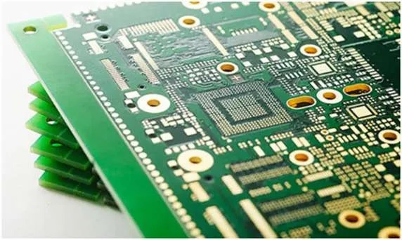
The decision between these different proto-PCB board types is influenced by a number of variables, such as the budget, space limitations, signal integrity requirements, and circuit design complexity. Engineers can choose the proto-board PCB that best fits their project objectives by being aware of the distinctive qualities of each type. This will help to ensure a seamless transfer from concept to reality.
Process of Designing Prototype Circuit Board:
The proto-circuit board design process converts an abstract circuit design into a functional physical prototype using planned steps. This method requires precision, attention to detail, and proper tools to ensure the final product meets expectations.
The process begins with creating a schematic diagram, which outlines connections and electrical properties as the circuit’s blueprint. The schematic guides the layout design, determining part placement and trace routing on the proto-board PCB.
Layout design involves converting the schematic into a physical layout, considering manufacturability, power, thermal, and signal integrity. Modern design software simplifies PCB creation by providing tools for schematics, layouts, and simulations, reducing errors and time.
Popular tools like Eagle, OrCAD, Altium Designer, and KiCad streamline design, modeling, and team collaboration. From concept to reality, proto-circuit board design ensures ideas become accurate, functional, and ready for product development.
Manufacturing Process for Prototype Circuit Boards:
Proto-circuit board manufacturing is a complex process that entails a number of phases that work together to turn a digital design into a working prototype.
The selection of materials is the first stage in the manufacturing process. The selection of the solder mask, copper cladding, and substrate material greatly influences the board’s electrical, mechanical, and thermal characteristics. The application, the operating environment, and financial limitations are all considered throughout the choosing process.
The etching procedure starts as soon as the materials are chosen. The circuit design is transferred onto the copper-clad substrate material using photolithography or laser imaging techniques. The intended conductive routes that will link the different components on the board are then left in place after the unneeded copper is removed using an etching tool.
Drilling and plating are crucial processes in the manufacturing process. Vias and component leads are drilled into the board to allow connections between the various layers. Copper is then plated into these holes to guarantee both mechanical strength and electrical conductivity.
The last steps in the manufacturing process involve soldering components onto the board, putting on a protective solder mask, and carrying out extensive testing to guarantee functioning and dependability. The entire production process necessitates a blend of cutting-edge technology and expert craftsmanship to guarantee that every proto-circuit board satisfies the exacting standards of the electronics sector.
SMT (Surface Mount Technology) in Proto-board Circuit Boards:
The mounting of electronic components on proto-circuit boards has been completely transformed by Surface Mount Technology (SMT), which has several benefits in terms of performance, efficiency, and downsizing. Because of this technique, tiny and potent gadgets can now be made. It has become the cornerstone of modern electronics manufacturing.
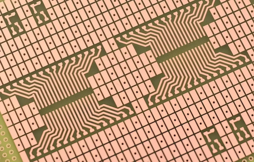
SMT components do not require drilling holes because they are made to be placed directly onto the proto express PCB surface, in contrast to their through-hole equivalents. Because these parts are usually lighter and smaller, the board size can be decreased, and the component density can be raised. Because of their shorter lead times and lower levels of parasitic effects, they also provide better electrical performance.
There are multiple crucial steps in the SMT assembly process. The PCB pads where the components are going to be installed first receive a solder paste application. Then, using automated pick-and-place devices, the parts are positioned precisely onto the pads. After that, the board is heated to a temperature that solidifies and forges a robust mechanical and electrical link with the components.
Because of all of its advantages, SMT has emerged as the standard technique for constructing proto-board PCBs. It makes it possible to design electronic devices that are lighter, more compact, and more effective. SMT assembly is a great option for low-volume production runs and prototyping because of its automation, which also improves consistency and speeds up production.
PCB Proto-board Through-hole Technology (THT):
Even though it was developed before Surface Mount Technology, Through-Hole Technology (THT) is still a useful and applicable technique for putting proto-circuit boards together, particularly in specific situations. It has clear benefits in terms of resilience, rework-friendliness, and compatibility with particular component kinds.

As the name suggests, THT components have leads that are entered through drilled PCB holes. Then, these leads are soldered to pads on the other side of the board to form a robust electrical and mechanical connection. Generally speaking, THT components are larger than their SMT equivalents, which makes them simpler to handle and rework by hand. This is especially useful while prototyping.
There are multiple crucial steps in the THT construction process.
The component leads are first put through the PCB’s pre-drilled holes. In order to guarantee correct alignment and avoid shorts, the leads are then bent and cut. After that, the board is sent through a wave soldering machine, which creates solder junctions between the PCB pads and component leads by flowing molten solder over the board’s bottom side.
Proto-board PCB assembly using THT is still a feasible solution, particularly for bigger component projects, high-power applications, or scenarios where flexibility in prototyping and manual rework are essential. THT is still a useful tool for electronics engineers and enthusiasts, even if SMT has taken the lead in today’s electronics manufacturing industry. THT is still useful in some applications.
Hybrid PCB Assembly Methods for Prototype boards:
A flexible method that combines the advantages of Through-Hole Technology (THT) and Surface Mount Technology (SMT) on a single board is a hybrid proto-board PCB assembly. More component placement and selection freedom are provided by this method, which also maximizes performance and meets a variety of design criteria.
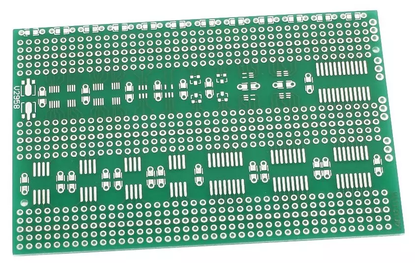
Utilizing the benefits of both technologies, engineers can combine SMT and THT on a proto-board PCB. THT components can be used for larger, heavier components or those that need to be manually adjusted and replaced during prototyping, whereas SMT components are best suited for high-density areas and fine-pitch devices. Greater adaptability and design freedom are made possible by this hybrid approach.
However, hybrid assemblies have additional difficulties. Handling both SMT and THT components increases the complexity of the manufacturing process and requires certain tools and knowledge. Component location and routing must also be carefully considered to prevent interference and guarantee signal integrity.
Hybrid proto-board PCB assembly techniques are still useful in many different fields despite these obstacles. When a variety of component sizes, technologies, and functionalities are needed for a project, they are especially helpful. Hybrid assemblies provide a flexible option for intricate and demanding electronic designs found in anything from medical devices and telecommunications equipment to industrial automation and vehicle electronics.
Assembly of Proto-board PCBs with Quality Control:
When it comes to proto-board PCB assembly, quality control is crucial to ensuring the finished product meets specifications and functions as intended. This involves rigorous tests and inspections to identify and address flaws or deviations from design parameters.
Proto-board PCBs undergo inspections using X-ray, automated optical inspection (AOI), and visual methods. Skilled technicians visually check for obvious flaws like damaged traces, misplaced components, or solder bridges. AOI uses high-resolution cameras and image processing to detect faults quickly and accurately. X-ray inspection examines internal layers and hidden solder joints, ensuring the entire board’s integrity.
Testing methods for proto-board PCBs include in-circuit testing (ICT), flying probe testing, and functional testing. Functional testing confirms the board performs as specified. ICT applies test signals to specific points, identifying malfunctioning parts or connections. Flying probe testing provides flexibility for intricate and densely packed boards, using probes to access test spots.
Common proto-board PCB flaws include solder bridges, open circuits, misplaced components, and cold solder joints. These defects can cause malfunctions, poor performance, or complete failure. Rework methods such as component replacement, reflow soldering, and hand soldering address these issues. Robust quality control during assembly minimizes errors and ensures the durability and reliability of the final product.
By combining advanced inspection techniques, thorough testing, and effective rework processes, proto-board PCB assembly ensures high-quality results while addressing potential defects efficiently.
Tools and Equipment for Assembly of Prototype PCB:
A variety of specialized tools and equipment are needed for proto-board PCB assembly; these tools and equipment are essential to turning a bare board into an operational electronic circuit. By enabling accurate component placement, trustworthy soldering, and comprehensive inspection, these instruments guarantee the end product’s quality and functionality.
Accurately inserting surface mount components onto the PCB requires picking and positioning machines. These automated devices pick up parts from reels or trays using suction nozzles or grippers, then quickly and precisely arrange them onto the appropriate pads. They greatly shorten assembly times and increase placement precision, particularly for intricate and heavily loaded boards.
The PCB pads and component leads are joined mechanically and electrically using soldering tools. This includes wave soldering machines for THT assembly, reflow ovens for SMT assembly, and soldering irons for manual soldering. The type of component and the assembly method being used determine which soldering equipment is best.
In order to find any flaws or departures from the design criteria, inspection instruments are essential. These instruments include automated optical inspection (AOI) systems, microscopes, and magnifying glasses. They make it possible to closely inspect the board and see problems like cold solder joints, misplaced parts, and solder bridges.
The tools and equipment must be chosen carefully and used appropriately to achieve high-quality proto-board PCB assembly. Manufacturers may guarantee the performance and dependability of their proto-board PCBs by making the appropriate tool investments and hiring qualified specialists, opening the door for fruitful product development and innovation.
Environmental Factors in the Assembly of Proto PCBs:
Proto-board PCB manufacturing is not an exception to the electronics industry’s growing emphasis on environmental issues. Proto PCB producers use eco-friendly materials and sustainable procedures to reduce their environmental effects as much as possible during the production process.
An essential component of environmentally friendly proto-board PCB assembly is waste management. This entails putting in place appropriate protocols for getting rid of dangerous substances and materials that are employed in production. It also means reducing the amount of waste produced by recycling and using materials more wisely.
PCB recycling is an additional crucial factor. There is less need to extract raw materials and less waste going to landfills because many of the parts and materials used to make PCBs may be recycled or recovered. A growing number of proto PCB manufacturers are collaborating with recycling centers to guarantee the appropriate disposal and retrieval of precious materials.
Proto-board PCB assembly is seeing an increase in the usage of environmentally friendly components. Choosing halogen-free laminates, biodegradable packaging materials, and lead-free solder are a few examples of this. These materials help create a more sustainable electronics industry by lessening the production process’s negative environmental effects.
Manufacturing companies of proto-board PCBs can significantly contribute to environmental protection by adopting sustainable processes and giving eco-friendly materials a priority. This is advantageous for the environment as well as for the business’s reputation and ability to draw in eco-aware clients.
Advances in Proto-board Assembly:
Proto-board PCB assembly evolves constantly, driven by technology advancements and the pursuit of innovative solutions in electronics manufacturing. Emerging technologies, materials, and methods are transforming how we design and produce electronic prototypes for diverse applications.
Advancements in materials enable more sustainable and efficient proto-board PCBs with improved thermal and electrical performance. New substrate materials allow greater design flexibility, miniaturization, and enhanced durability for cutting-edge electronic designs. Recyclable and bio-based materials are gaining popularity, reducing the environmental impact of proto-board PCB production.
Innovative assembly methods promise faster turnaround times and higher accuracy in PCB manufacturing. Rapid prototyping with 3D printing enables custom boards with complex features in just a few hours.
Laser direct structuring (LDS) creates conductive traces on 3D-printed objects, expanding design possibilities significantly. Artificial intelligence (AI) and machine learning (ML) streamline workflows, optimize designs, and reduce errors in PCB production. The Internet of Things (IoT) drives demand for compact, efficient, and interconnected proto-board PCBs.
These advancements support faster iterations, better sustainability, and improved design adaptability in electronics development. Staying updated with innovations ensures engineers and manufacturers push boundaries and remain leaders in the electronics field.
Catalyst for Innovation:
Proto circuit boards are the catalysts for invention that help engineers and designers realize their visions, serving as more than just steppingstones in the product development process.
It takes a lot of work and complexity to go from a conceptual circuit design to a physical, working prototype. The vital link between these two domains is provided by proto-circuit boards.
The boards allow engineers and designers to experiment, improve, and verify their concepts prior to going into large-scale manufacturing. They are essential in shortening timeframes for product development, cutting expenses, and guaranteeing that the finished product fulfills the highest requirements for performance and quality.
Advantages of Prototype Circuit Boards:
Design Validation
Helps test and refine the circuit design before full-scale production.
Identifies and resolves potential flaws early in the process.
Cost-Effective
Saves money by avoiding costly mistakes in mass production.
Inexpensive materials like breadboards or perfboards can be used initially.
Quick Iteration
Allows rapid testing and modifications to improve the design.
Shortens the development cycle by enabling real-time changes.
Customization
Supports unique designs tailored for specific applications or needs.
Offers flexibility in trying out different configurations.
Learning and Education
Useful for teaching electronics and practical skills to students and hobbyists.
Encourages innovation and hands-on experimentation.
Proof of Concept
Demonstrates the feasibility of a design to stakeholders or investors.
Provides a working model to gather feedback.
Risk Mitigation
Reduces risks by ensuring the circuit functions as intended before scaling production.
Disadvantages of Prototype Circuit Boards:
Time-Consuming
Building and testing prototypes can take significant time, especially for complex designs.
Limited Durability
Prototypes often use temporary or fragile materials, making them unsuitable for long-term use.
Higher Initial Effort
Requires detailed planning, designing, and testing, which can be labor-intensive.
Potential Errors
Manual assembly and testing may lead to mistakes, especially in complex circuits.
Not Production-Ready
Prototypes may not meet manufacturing or industry standards for mass production.
Material and Performance Limitations
Breadboards or Protoboards may not accurately represent the final PCB’s performance characteristics.
Cost in Advanced Prototypes
Custom PCBs or advanced prototyping techniques can be expensive compared to basic methods.
By balancing these advantages and disadvantages, prototype circuit boards are an invaluable tool for engineers, students, and innovators in developing and perfecting electronic designs.
Applications Prototype Circuit Board:
A prototype circuit board is used to test and develop electronic designs before final production. Here are some common uses:
1. Product Development
Test new gadgets like phones, IoT devices, or sensors. Fix problems early in the design.
2. Education
Learn electronics using tools like Arduino or Raspberry Pi. Build simple circuits for school or personal projects.
3. Research
Create and test experimental tech, like medical devices or robotics. Quickly try out new ideas.
4. DIY Projects
Build custom devices like smart home gadgets or unique tools. Solve personal or small-scale problems.
5. Pre-Production
Double-check a design before mass production. Ensure it works well and is easy to manufacture.
6. Embedded Systems
Test small computers like microcontrollers (used in robots or sensors). Build modular systems that can be programmed and improved.
7. Proof of Concept
Show how a device will work to investors or teammates. Use it as a working demo for feedback.
Conclusion:
Proto-board PCB assembly technology is developing at an advanced rate. The limits of what is feasible are continuously being pushed by the continuous development of new materials, assembly methods, and design tools.
The field’s future is being shaped by the convergence of AI and ML, the Internet of Things, and the growing emphasis on sustainability. These developments are expected to further boost innovation and efficiency in the electronics sector.
The ability to grasp the complexities of proto-board PCBs and welcome new developments will enable us to push the limits of electronics and create a future in which technology is seamlessly integrated into every part of our lives.
Revolutionary Axial Flux Printed Circuit Board (PCB) Stator Motor
