Let’s see NOR Gate Truth Table and its IC and various other logics implemented using this gate. logical NOR gate is a transistor-based electronic circuit, that produces a high output if all inputs are low.
My dear friends warmly welcome all of you devoted readers to yet another excellent article NOR Gate Truth Table. A NOR Gate is a combination of the logical OR Gate and logical NOT Gate. Since the NOT gate is added to the OR gate, therefore the output of the OR gate is inverted, also further we can say that the output of the OR gate is complemented by the NOT gate. or, to put it another way, a NOR gate is a negation of OR operators.
The Boolean expression of NOR gate is ![]()
The standard and most common definition to remember logically its operation is as follows 👇👇👇
“If all of the inputs are low then only output will be high”
or
“If all of the inputs are false, then only the output will be true.”
NOR Gate Truth Table-:
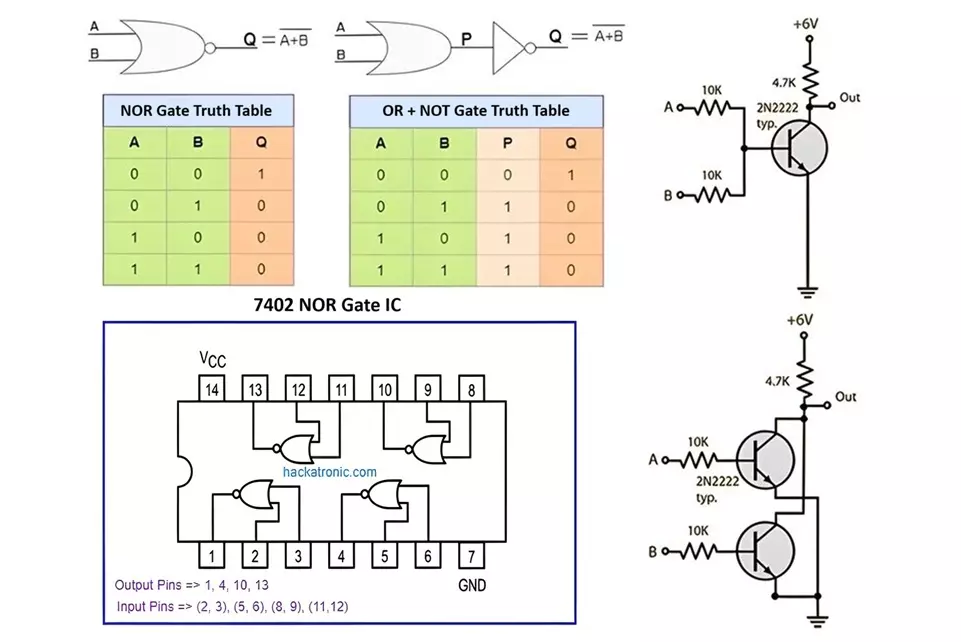
Dear friends let us check the symbol and truth table for NOR Gate with the below figure 1.
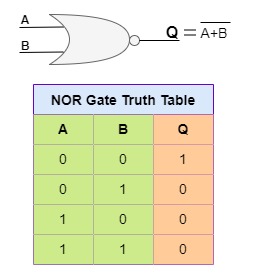
In above figure 1, the bubble at the tip of the OR gate symbolizes the NOT gate and reverses the output of the OR gate. in the below figure 2, you can see that output of the OR gate shown in the P column is reversed as shown in column Q after providing input to the NOT gate.
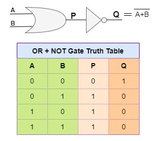
The Boolean expression for the OR gate is P = A+B and to represent the negation or NOT gate a bar (—-) is on the top of the A+B therefore the Boolean expression for the NOR gate is ![]()
Now you can check that if all the inputs are low then only the output goes to the high state otherwise it will remain in the lower state this validates our common standard definition. As we know that all types of logic gates such as AND, OR, NOT, NAND, XOR and XNOR can be constructed using transistor logic. Now let us understand the Transistor-Transistor Logic (TTL) logic for the NOR gate
TTL Logic for NOR Gate -:
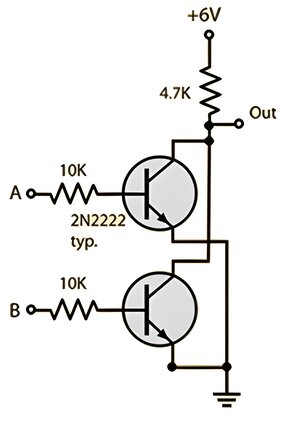
The utility of transistors as fast switches helps determine their use in the construction of logic gates. When the base-emitter diode is turned on sufficiently to drive it into saturation, the collector voltage concerning the emitter can be close to zero and used to construct gates for the TTL logic family.
The transistors are connected in parallel with the output, so if either or both of the inputs are high, the output is driven low. if any of the inputs are high then it will turn on the transistor resulting in the closed circuit or (we can say that a short-circuit provides a path to flow the current) and output is low. And if both transistors are supplied with low inputs, then they remain in the off state resulting in high voltage at the output terminal. As shown in the below figure 3
RTL Logic for NOR Gate -:
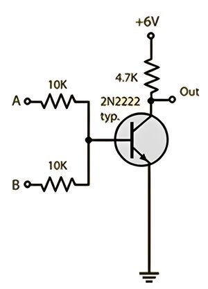
Only one transistor is used in this alternative method of achieving NOR logic, with the two inputs connected to its base via resistors. The output is driven low if either or both of the inputs are high.
7402 NOR Gate IC Pin Diagram:
The most commonly used IC for NOR gate is IC 74LS02, and its name is described as “7402 Quad 2-Input NOR Gate”, where 7402 is the model number and Quad indicates that four NOR gates are used, and each gate has 2 inputs as shown in the below image.
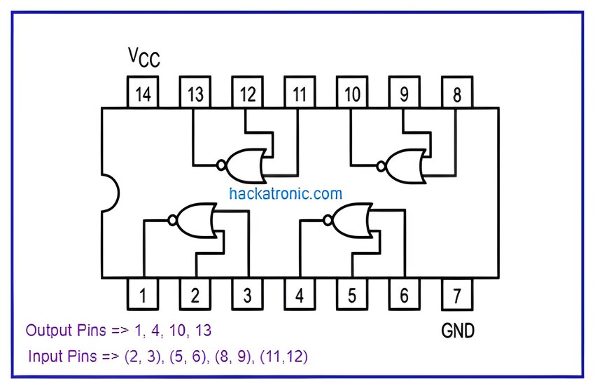
As mentioned in the above image 1, 4, 10, and 13 are the output pins, and (2, 3), (5, 6), (8, 9), and (11,12) are corresponding input pins for the output pins.
De-Morgan’s Law:
Before studying the NOR gate as a universal logic gate we need to understand the two basic fundamentals of the NOR gate which will be used while constructing other gates using NOR gate
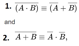
where:
- is the logical AND,
- is the logical OR,
NOR as a Universal Gate:
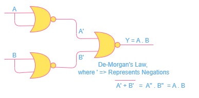
The NOR and NAND gates are known as universal gates because they can be used to build all types of logic gates, including the OR, NOT, AND, XOR, and XNOR. Below is an example of how we can construct the logical gates using NOR gate.
NOT Gate using NOR Gate:
A NOT gate is a simple logic gate with one input and one output. It is a logic gate with an output that is always the complement of its input. As a result, the NOT gate is also referred to as an inverter. If the NOT gate’s input is LOW (Logic 0), it produces a HIGH output (Logic 1). If the input is HIGH (Logic 1), the NOT gate outputs LOW (Logic 0).
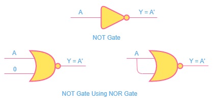
With help of the above logical diagram, we can verify the truth table of NOT gate
OR Gate Using NOR Gate:
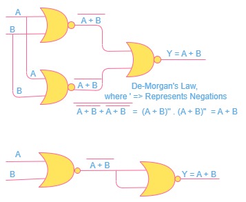
AND Gate Using NOR Gate:
What is Flip Flop Circuit? Types of Flip Flops with Truth Table
Types of Logic Gates with Symbol, Truth Table and IC Numbers
Universal NAND Gate Truth Table, Logic Circuit & IC 7400 Pin Diagram


Hi
This article is basic of digital electronics, and very much useful for digital electronic learners.
Good Job!