Explore Universal NAND Gate from its truth table to its IC pin diagram, delve into transistor-based logic circuit construction and working, and discuss the advantages, disadvantages, and various applications of the NAND gate. Just as the NOR gate combines the OR and NOT functions to provide an inverted output when all inputs are low, the NAND gate takes the AND operation and inverts its result. In simple terms, a it produces a low output only when all of its inputs are high.
What is a NAND Gate?
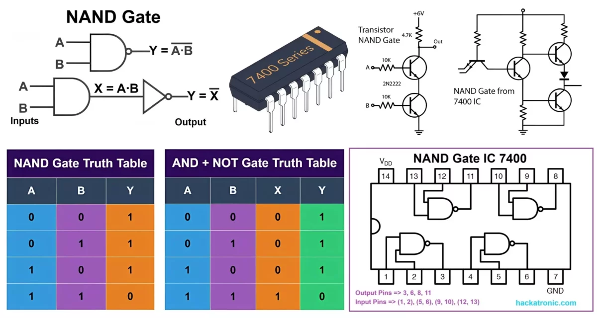
A NAND gate — short for NOT AND is a digital electronic circuit that outputs a low (0) only when every input is high (1). In all other cases, the output remains high (1).
Universal Nature of the NAND Gate
One of the most important properties of the NAND gate is its universality. This means that any other logic gate (AND, OR, NOT, XOR, XNOR, etc.) can be constructed using just NAND gates. This versatility makes it an invaluable component in digital electronics design, allowing for simpler circuit design and reduced component variety.
Symbol and Boolean Expression
The symbol for a NAND gate is similar to that of an AND gate with an additional small circle (representing the NOT operation) at the output.
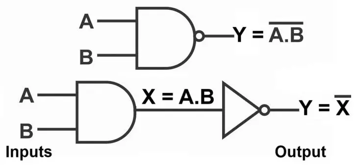
The Boolean expression for a two input NAND gate is written as:
Y = (A·B)’
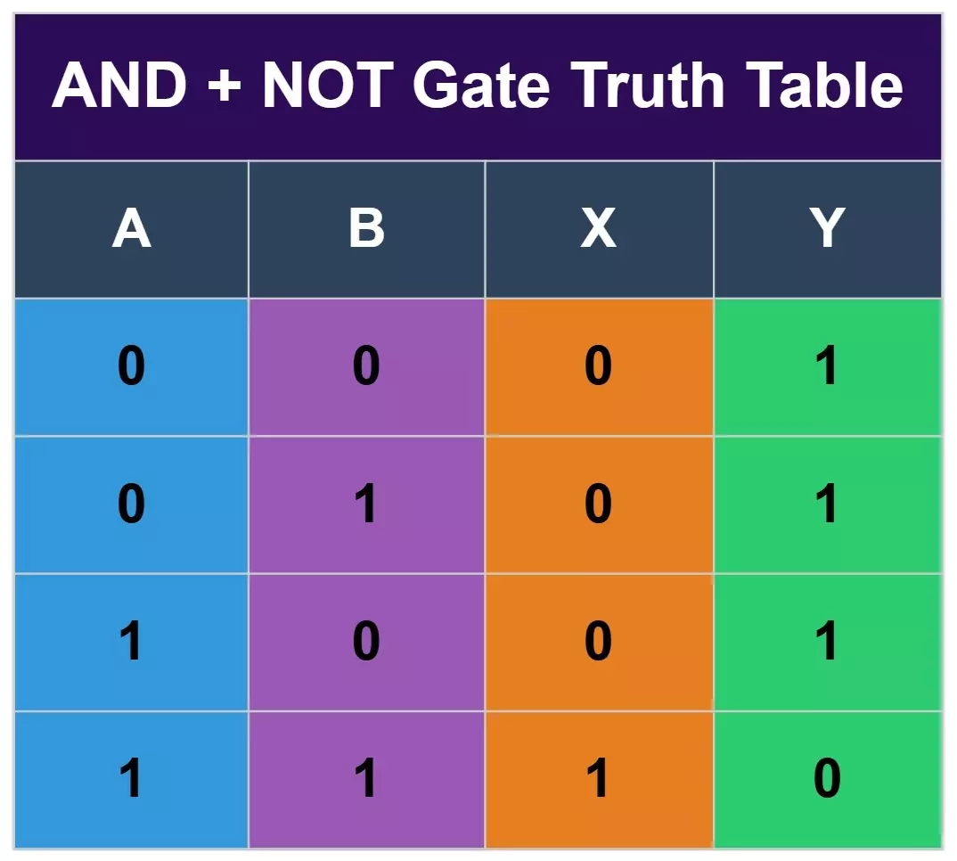
This means that the NAND gate is essentially an AND gate followed by a NOT gate, which complements the output of the AND operation.
NAND Gate Truth Table
Let’s take a look at the truth table for a 2-input NAND gate:
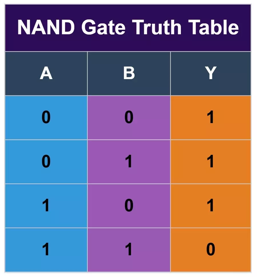
The standard and most common definition to remember its operation is as follows:
“If all of the inputs are high, then only the output will be low.”
For n-input NAND gates, the output will be low only when all inputs are high; otherwise, the output is high.
NAND Gate TTL and RTL Logic Circuit
Here is an overview of both RTL and TTL NAND gate logic circuits, highlighting their design and operational differences.
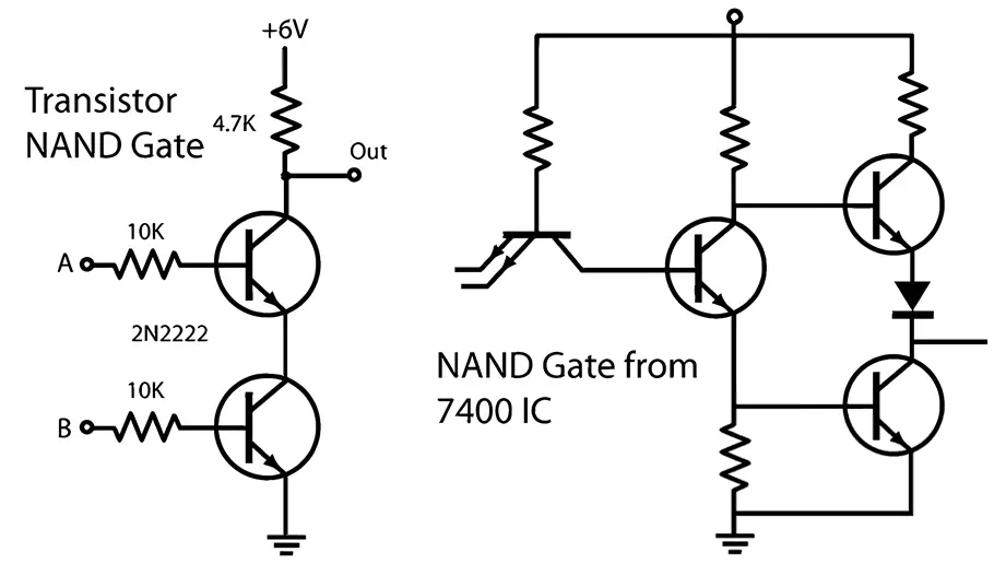
NAND Gate RTL Logic Circuit
Resistor-Transistor Logic (RTL) is one of the earliest logic families. In an RTL NAND gate:
- Structure:
Two NPN transistors are connected in series with a resistor acting as a pull-up to the supply voltage.- Inputs: Each input is applied directly to the base of its respective transistor.
- Output: Taken from the junction between the series transistors and the resistor.
- Operation:
- Both Inputs High: When both transistor bases are driven high (sufficient base-emitter voltage), both transistors saturate (conduct), forming a low-resistance path to ground. This pulls the output voltage low (logic 0).
- Either Input Low: If at least one input is low, its transistor remains off (non-conducting). This breaks the series conduction path so the pull-up resistor pulls the output high (logic 1).
- Key Points:
- RTL is simple and economical but tends to be slower with lower noise margins compared to later logic families.
- The resistor sets the logic “high” level and influences current flow, making RTL designs sensitive to loading effects.
NAND Gate TTL Logic Circuit
Transistor-Transistor Logic (TTL) evolved to overcome some of the limitations of RTL. In a TTL NAND gate:
- Structure:
- Input Stage: A multi-emitter transistor is typically used for the inputs. This transistor can “steer” current based on the voltage level of each input.
- Phase-Splitting Stage: An additional transistor stage helps generate complementary signals needed to drive the output stage.
- Output Stage: Often implemented as a totem-pole (or push-pull) configuration. Two output transistors work in anti-phase—one sourcing current and the other sinking current—to actively drive the output to either a high or low level.
- Operation:
- Both Inputs High: When all inputs are high, the multi-emitter transistor’s base–emitter junctions are reverse-biased. This allows enough current to flow into the subsequent stage, ultimately turning the output transistor on and pulling the output low.
- Any Input Low: If one (or more) input is low, current steering causes the base of the next transistor stage to be pulled toward ground. This prevents the output transistor from turning on, so the pull-up in the totem-pole stage drives the output high.
- Key Advantages:
- Speed: The use of multiple transistor stages (including a current-steering input and totem-pole output) reduces propagation delays.
- Noise Margin and Fan-out: TTL circuits provide better noise immunity and can drive more inputs (a higher fan-out) than RTL.
- Robustness: The totem-pole design actively drives both high and low states, ensuring faster and more reliable switching.
Comparison
- RTL NAND Gate:
- Simplicity: Fewer components (resistors and transistors)
- Performance: Slower, lower noise margin, and more sensitive to load variations
- Usage: Historical interest and simple educational circuits
- TTL NAND Gate:
- Complexity: More stages (multi-emitter input, phase-splitter, totem-pole output)
- Performance: Faster switching, better fan-out, and improved noise margins
- Usage: Widely used in classic IC families (e.g., 7400 series) and as building blocks for more complex digital circuits
Both TTL and RTL methods highlight the ease with which NAND gates can be implemented using transistor-based technology.
IC 7400 Quad 2 Input NAND Gate
The most commonly used integrated circuit for implementing NAND logic is the IC 7400. This IC houses four independent 2-input NAND gates. Below is the typical pin diagram for the 7400 NAND gate IC:
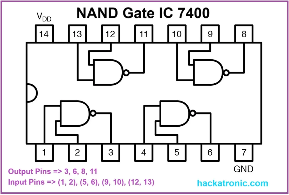
The 7400 IC is widely used in various digital circuits due to its robustness, low cost, and ease of integration.
De-Morgan’s Law and NAND Gate
Understanding De-Morgan’s Law is critical when working with universal gates like the NAND. “The complement of an OR operation is equal to the AND of the complements.” De-Morgan’s Theorem for a NAND operation is given by:
(A · B)’ = A’ + B’
This means that a NAND gate can be viewed as an OR gate whose inputs have been inverted. Such transformations are fundamental when designing more complex digital circuits and when converting one type of logic gate to another.
Implementing All Other Logic Gates Using NAND Gates
Due to its universal nature, you can construct various other logic gates using only NAND gates:
NOT Gate Using a NAND Gate
A NOT gate (inverter) can be built by connecting both inputs of a NAND gate to the same signal:
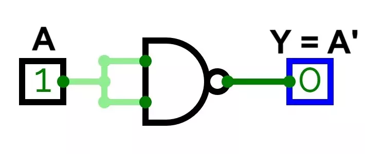
- Boolean expression: Y = (A·A)’ = A’
- When A is low, Y is high; when A is high, Y is low.
AND Gate Using NAND Gates
An AND gate can be realized by first using a NAND gate and then inverting its output:
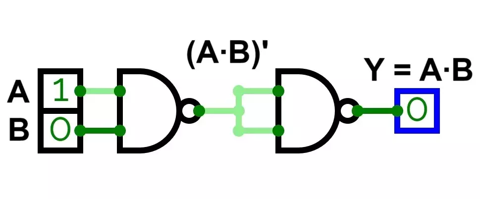
- First, compute (A·B)’ using a NAND gate.
- Then, invert it using another NAND gate configured as a NOT gate.
- Boolean expression: AND = A·B
OR Gate Using NAND Gates
By applying De-Morgan’s Theorem, an OR gate can be constructed using three NAND gates:
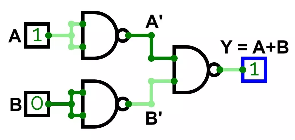
- First, compute A’ = (A·A)’ using a NAND gate as a NOT gate.
- Then compute B’ = (B·B)’ using another NAND gate as a NOT gate.
- Next, compute OR = (A’·B’)’ using a NAND gate (this gives A + B).
- Boolean expression: OR = (A’·B’)’ = A + B
NOR Gate Using NAND Gates
A NOR gate can be constructed using four NAND gates:
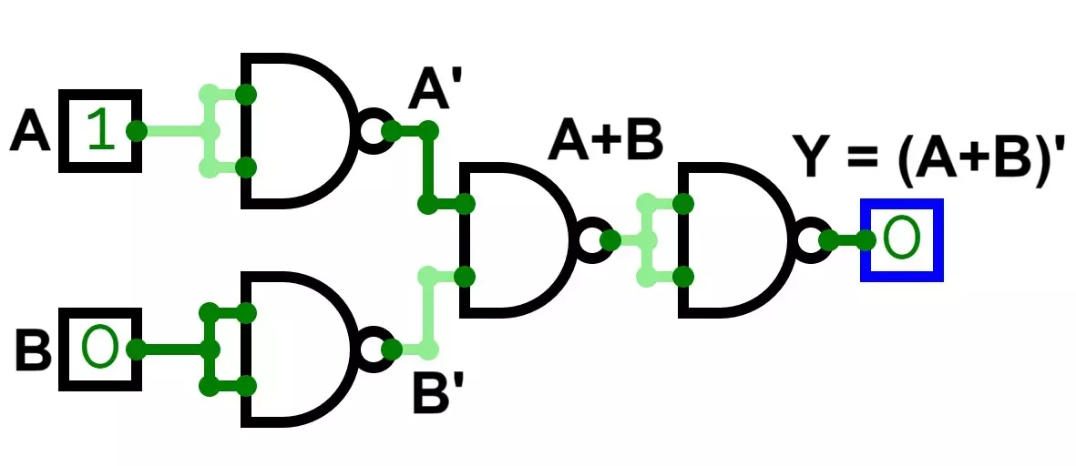
- First, invert both inputs using NAND based inverters.
- Then, feed these inverted signals into a NAND gate.
- Finally, invert the OR output to get NOR: NOR = (OR·OR)’
- Boolean expression: NOR = ((A’·B’)’)’ = (A + B)’
XOR Gate Using NAND Gates
An XOR gate can be realized using a combination of four NAND gates:
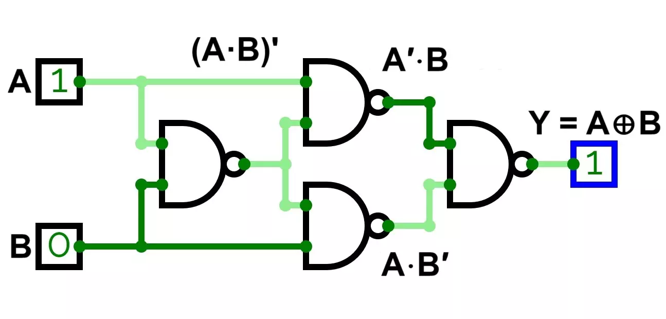
- First, compute (A·B)’ using a NAND gate.
- Then compute (A·(A·B)’)’ using a NAND gate.
- Compute (B·(A·B)’)’ using another NAND gate.
- Finally, compute XOR = ((A·(A·B)’)’ · (B·(A·B)’)’)’, which gives the XOR output.
- Boolean Expression: XOR = ((A·(A·B)’)’ · (B·(A·B)’)’)’ = A ⊕ B
XNOR Gate Using NAND Gates
An XNOR gate can be built by inverting the output of the XOR gate, it is constructed from 5 NAND gates:
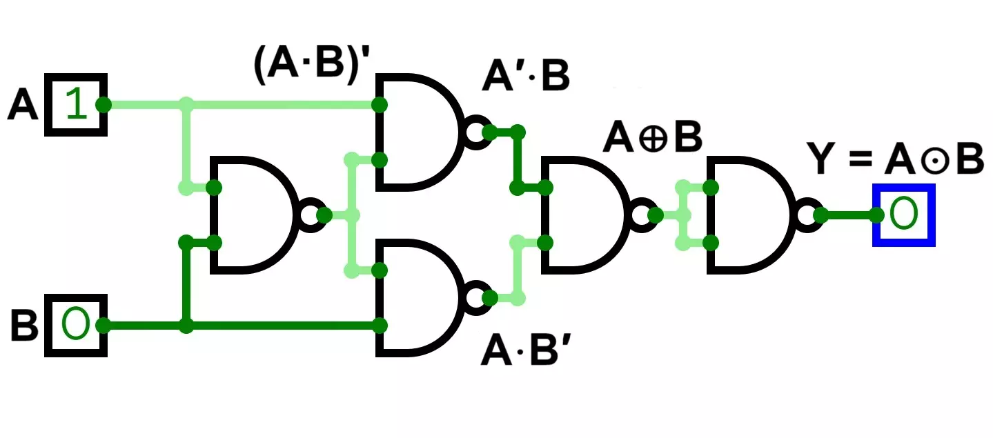
- First, construct XOR as described above.
- Then, invert the XOR output using a NAND gate configured as a NOT gate:
XNOR = (XOR·XOR)’ - Boolean Expression: XNOR = (A ⊕ B)’ = A ⊙ B
Advantages of NAND Gates
- Universality: As mentioned earlier, NAND gates can be used to construct any other logic gate. This simplifies the design process and inventory management in digital circuit design.
- Cost-Effective: With a simpler design and lower manufacturing costs, NAND gates are economical for large-scale production.
- Reduced Component Count: Relying on one type of gate for multiple functions can streamline circuit layouts and minimize the number of different components required.
- High-Speed Operation: NAND gates are typically fast, which makes them suitable for high-speed digital applications.
- Low Power Consumption: In many cases, NAND gates can be designed to consume less power compared to more complex logic circuits.
Disadvantages of NAND Gates
- Complexity in Large Systems: While a NAND-only design is elegant in theory, using NAND gates to implement every function in a complex circuit can lead to increased circuit complexity and a larger number of gates.
- Propagation Delays: Each gate introduces a small delay in signal processing. In very high-speed circuits, these delays can add up and affect overall performance.
- Power Consumption in High-Density Circuits: In densely populated circuits with many gates, the cumulative power consumption might become a concern, especially in battery-operated devices.
Applications of NAND Gates
NAND gates find applications in a wide variety of digital systems, including:
- Digital Logic Circuits: The fundamental building block for creating AND, OR, NOT, XOR, and other logic circuits.
- Computers and Microprocessors: Used extensively in the design of ALUs, memory systems, and control units.
- Memory Devices: NAND Flash memory is a cornerstone of modern storage devices such as SSDs, USB drives, and memory cards.
- Control Systems: Employed in embedded systems for signal processing, decision making, and control logic.
- Sequential Logic: Integral in designing flip-flops, counters, and registers where timing and state retention are crucial.
- Error Detection and Correction: Used in implementing circuits that detect and correct errors in data transmission and processing.
Conclusion
In summary, the Universal NAND Gate is a versatile and essential component in digital electronics. With its simple yet powerful operation — outputting low only when all inputs are high — it serves as the foundation for constructing all other types of logic gates. From its transistor-based TTL and RTL implementations to its integration in the popular 7400 IC, the NAND gate’s efficiency, cost-effectiveness, and speed make it indispensable in everything from simple logic circuits to advanced computing systems. The CMOS version of NAND IC 7400 is CD4011. By understanding its truth table, Boolean expressions, and methods of constructing complex logic functions, engineers and students alike can harness the full potential of the NAND gate in their designs.
Types of Logic Gates with Symbol, Truth Table and IC Numbers
Half Adder and Full Adder Circuit, Truth Table, Equation with IC 7483
What is Flip Flop Circuit? Types of Flip Flops with Truth Table
