A TVS (Transient Voltage Suppression) diode is a specialized semiconductor device used to protect electronic circuits from high-voltage transients such as electrostatic discharge (ESD), lightning surges, and switching spikes. It responds extremely fast and clamps overvoltage to a safe level before they damage sensitive components.
Modern electronic systems are highly sensitive to voltage spikes caused by high-speed switching, inductive loads, lightning, and power line disturbances. These spikes may last only nanoseconds or microseconds but are often large enough to damage ICs, microcontrollers, and communication interfaces.
To prevent such damage, TVS diodes are widely used for surge protection. They clamp transient voltages, divert excess current, and then automatically return to their normal state, providing reliable and continuous circuit protection.
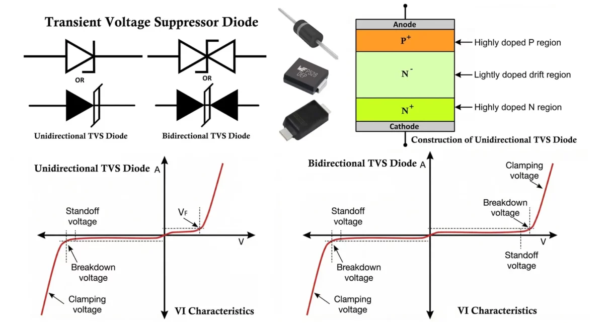
Symbol of TVS Diode
The symbol of a TVS diode resembles a Zener diode, but it is specifically optimized for transient suppression.
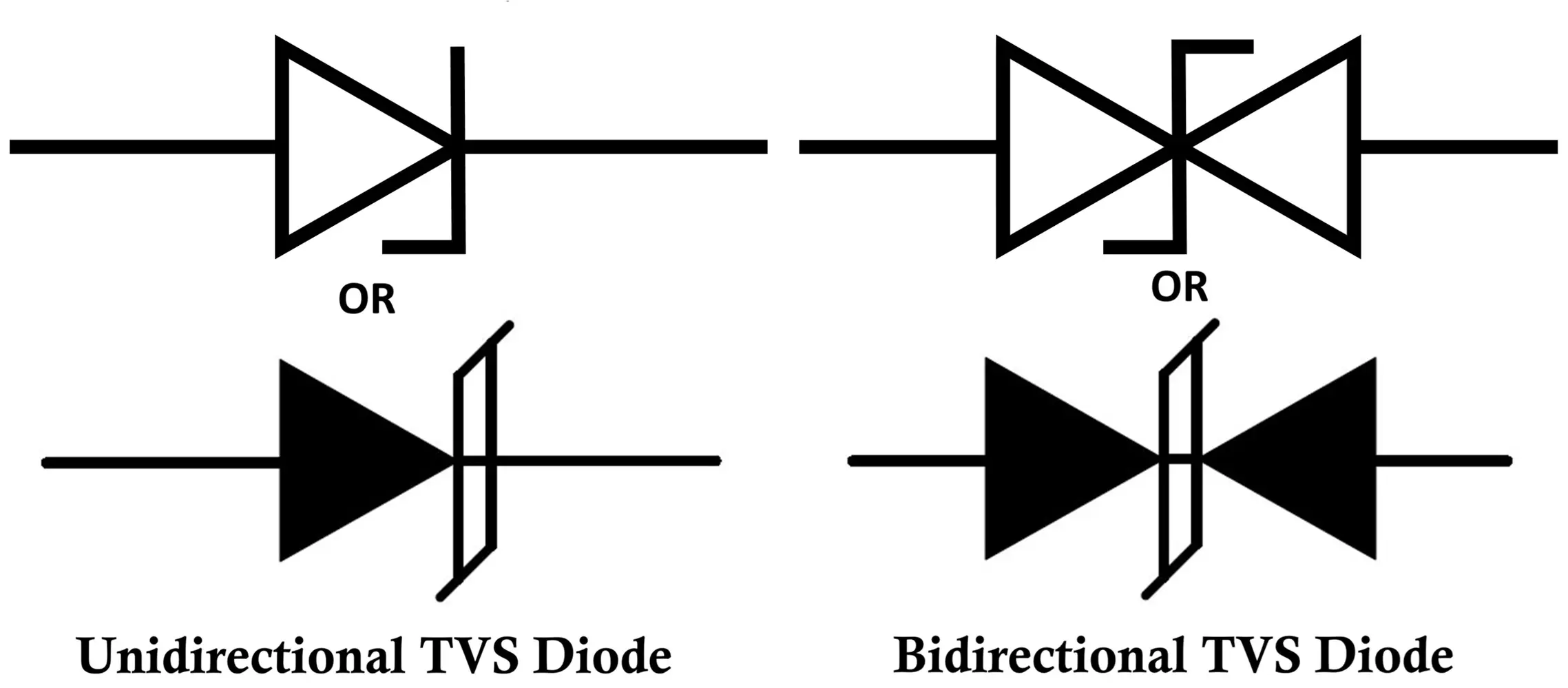
- Unidirectional TVS Diode Symbol: It looks like a Zener diode and conducts only in reverse breakdown during overvoltage.
- Bidirectional TVS Diode Symbol: It looks like two Zener diodes connected back-to-back and can clamp both positive and negative transients.
Construction of TVS Diode
The basic structure of a TVS diode employs a heavily optimized PN junction that operates in the avalanche breakdown region without suffering damage. The construction emphasizes high surge current handling, fast response time, and thermal stability.
Internally it resembles a planar Zener / avalanche diode, but with much larger junction area and special edge termination for high reliability.
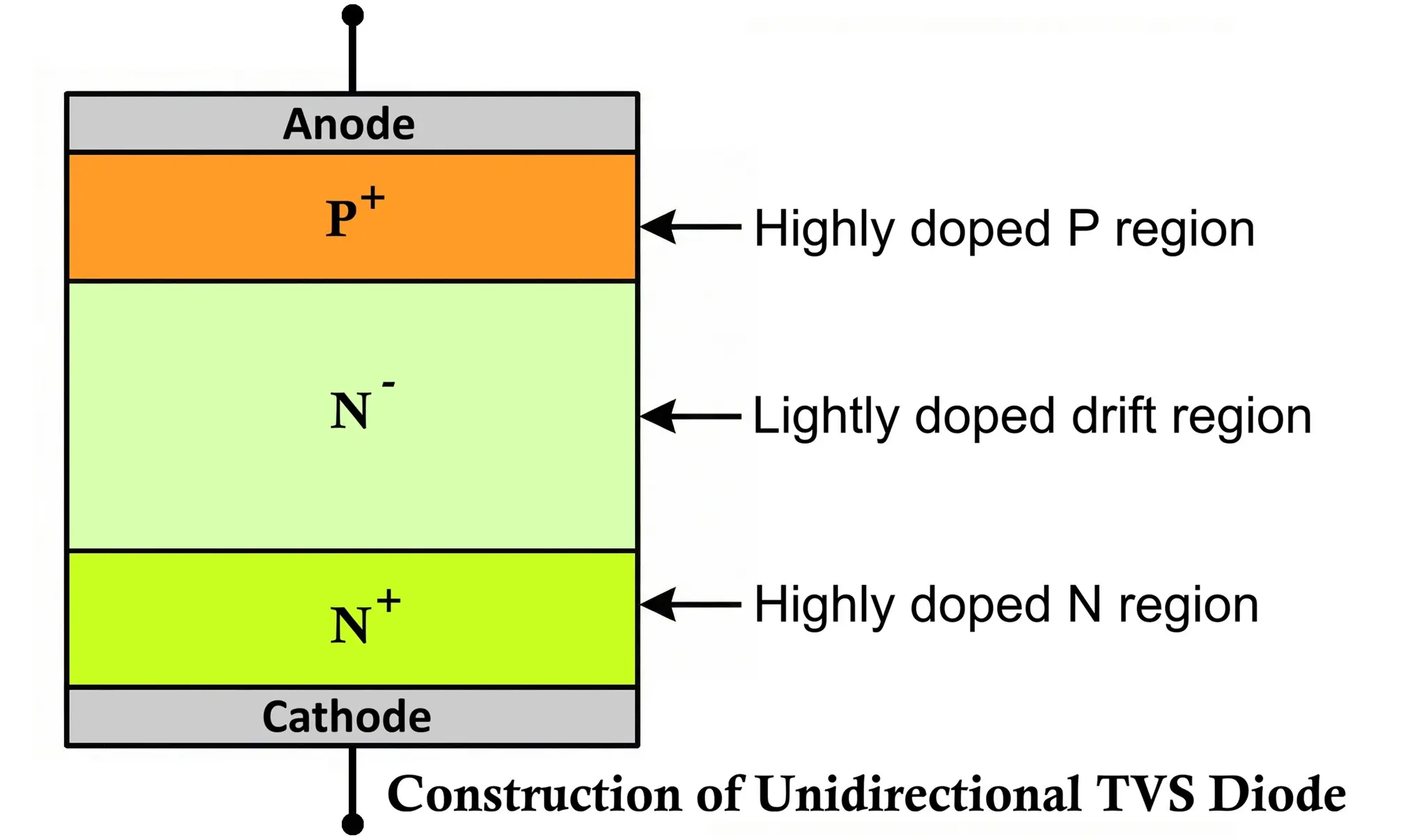
- Unidirectional TVS Diode (P+ N- N+ structure)
- Internal structure of a unidirectional TVS diode is shown above.
- Bidirectional TVS Diode (N+ P- P+ structure)
- A bidirectional TVS is effectively two diodes in anti-series on the same die in a symmetrical structure.
Internal Structure
P-type Semiconductor Layer
The P-type layer contains holes as the majority charge carriers. It is heavily doped to reduce internal resistance and allow large transient currents to flow safely during a surge event.
N-type Semiconductor Layer
The N-type layer contains electrons as the majority carriers. Like the P-layer, it is also heavily doped to provide low resistance and high current conduction capability.
Drift Region (Lightly Doped Region)
Between the heavily doped P and N layers lies a lightly doped drift region. This region determines the breakdown voltage of the TVS diode. When the applied voltage exceeds the rated breakdown voltage, this region undergoes controlled avalanche breakdown, allowing excess energy to be diverted safely away from the protected circuit.
During a transient event, the strong electric field in the drift region causes impact ionization, creating a large number of charge carriers. This process allows the diode to conduct heavily and clamp the voltage at a predetermined level.
Physical Construction
The P-type and N-type semiconductor layers are fabricated on a large-area silicon die to distribute current and heat evenly. Compared to ordinary signal or Zener diodes, the TVS diode has:
- A much larger junction area for high power dissipation
- Thicker metal contacts for low electrical resistance
- A robust structure optimized for repetitive surge events
Anode and Cathode Contacts
The anode and cathode contacts are formed using thick metal layers, usually aluminum or copper, deposited on the top and bottom surfaces of the silicon chip. These contacts ensure low-resistance current flow during surge conduction and also act as heat spreaders.
In bidirectional TVS diodes, two identical avalanche diodes are connected back-to-back on a single silicon substrate, allowing the device to suppress both positive and negative voltage transients.
Passivation and Protection Layers
The surface of the silicon chip is coated with a passivation layer such as silicon dioxide (SiO₂) or silicon nitride (Si₃N₄). This layer:
- Protects the junction from moisture and contamination
- Improves long-term stability
- Prevents surface leakage currents and breakdown shifts
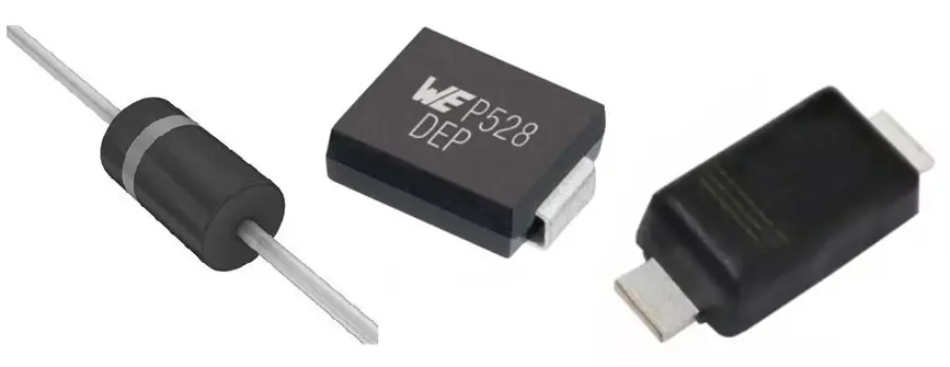
Encapsulation and Packaging
To protect the semiconductor and ensure mechanical reliability, the TVS diode is encapsulated in a high-strength epoxy or molded plastic package. Common package types include axial leaded (DO-15, DO-201) and surface-mount packages (SMBJ, SMCJ, SMDJ).
The package is designed to:
- Withstand high temperatures during surge events
- Provide low thermal resistance for heat dissipation
- Minimize lead inductance for fast transient response
Materials Used in TVS Diodes
TVS diodes are primarily manufactured from high-purity silicon because of its stable breakdown characteristics and excellent thermal performance. In specialized high-speed or RF protection applications, silicon carbide (SiC) or other advanced materials may be used.
Key Construction Features:
A TVS diode is optimized to absorb high transient energy safely.
- Silicon-Based P-N Junction
TVS diodes are made from silicon and heavily doped to achieve precise breakdown voltage and fast response. - Large Junction Area
The junction area is significantly larger than that of signal diodes or Zener diodes, allowing it to handle large surge currents. - Optimized for Avalanche Breakdown
The junction is engineered to operate safely in the avalanche region without degradation. - Low Junction Capacitance (for data lines)
Special low-capacitance TVS diodes are used for high-speed communication lines to avoid signal distortion. - Encapsulation
TVS diodes are available in:- DO-214 (SMBJ, SMCJ)
- SOD-123
- SOT-23
- SMT and THT packages
Working of TVS Diode
It operates on the principle of avalanche breakdown and responds very fast to voltage spikes from lightning, electrostatic discharge (ESD), and inductive switching.
Normally, the TVS diode remains in a high-impedance state. When the voltage exceeds its breakdown level, it switches to a low-impedance state, conducts, and diverts excess energy to ground, clamping the voltage. After the transient, it returns to its non-conducting state.
Voltage Regions
- Below Breakdown Voltage:
- The TVS diode remains in its off-state and draws negligible current.
- At Breakdown Voltage:
- The strong electric field across the junction causes impact ionization, initiating avalanche breakdown.
- Above Breakdown Voltage:
- The diode conducts heavily, clamping the voltage and absorbing the surge energy.
Modes of Operation
1. Normal Operation (No Surge Condition)
When the voltage across the TVS diode is below its rated breakdown voltage:
- The diode remains reverse-biased.
- Only a very small leakage current flows.
- The TVS diode behaves like an open circuit and does not interfere with normal circuit operation.
Thus, during normal voltage conditions, the TVS diode is electrically invisible to the system.
2. Surge Condition (Transient Event)
When a sudden voltage spike appears:
- The voltage rises rapidly beyond the breakdown level of the TVS diode.
- The electric field in the junction becomes very strong.
- Impact ionization occurs, generating electron-hole pairs.
- The diode enters avalanche breakdown and becomes highly conductive.
- The surge current is diverted through the TVS diode instead of passing into sensitive components.
- The voltage across the protected circuit is clamped to a safe maximum value.
This entire process occurs in a few picoseconds to nanoseconds, allowing extremely fast protection.
3. Recovery After Surge
Once the transient voltage disappears:
- The voltage falls back below the breakdown level.
- The avalanche process stops.
- The diode returns automatically to its high-impedance state.
- Normal circuit operation resumes.
The TVS diode can repeat this process many times without degradation if operated within its rated limits.
Unidirectional and Bidirectional Operation
Unidirectional TVS Diode
- Acts like a rectifier diode in forward bias and an avalanche diode in reverse bias.
- Used mainly in DC circuits.
Bidirectional TVS Diode
- Consists of two avalanche diodes connected back-to-back.
- Protects against both positive and negative voltage transients.
- Used in AC and data line protection.
VI Characteristics of TVS Diode
The VI characteristic of a TVS diode describes how the device responds to different voltage levels across its terminals. It shows that the TVS diode remains non-conductive (shows high resistance) during normal operation and becomes highly conductive (very low resistance) when a transient voltage exceeds its breakdown level, allowing it to clamp transient spikes effectively.
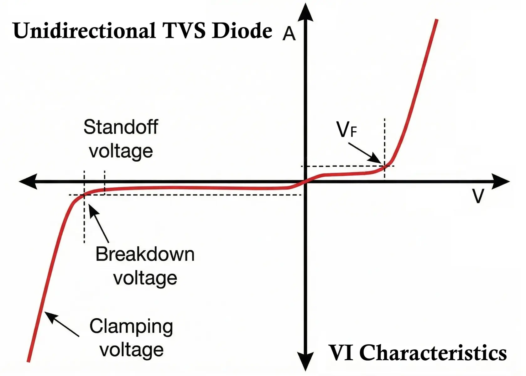
Regions of the VI Curve
1. Stand-off Region (Normal Operation)
- The applied voltage is below the rated stand-off voltage VR.
- The TVS diode is in a reverse-biased condition.
- Only a very small leakage current flow.
- The diode behaves like an open circuit and does not affect the system.
2. Breakdown (Avalanche) Region
- When the voltage reaches the breakdown voltage VBR, avalanche breakdown begins.
- Impact ionization generates a large number of charge carriers.
- The diode starts conducting heavily.
- The current increases sharply with only a small increase in voltage.
3. Clamping Region
- As the surge current increases, the diode limits the voltage to the clamping voltage VC.
- The excess current is diverted through the TVS diode.
- The protected circuit voltage remains nearly constant even though the surge current may be very high.
4. Recovery Region
- After the transient disappears, the voltage drops below VBR.
- The avalanche process stops.
- The diode returns to its high-impedance state.
Voltage Clamping Behavior
A TVS diode is characterized by three important voltage parameters:
- Breakdown Voltage (VBR):
The voltage at which the TVS diode begins avalanche conduction. - Clamping Voltage (VC):
The maximum voltage level that appears across the protected circuit during a surge. - Stand-off Voltage (VR):
The maximum continuous normal operating voltage that the TVS diode can withstand without conducting.
The device ensures that the circuit voltage never exceeds the clamping voltage during a transient.
The VI curve of a TVS diode has three regions:
- Leakage Region – below breakdown voltage, very small leakage current flows.
- Breakdown Region – at breakdown voltage, the diode conducts heavily.
- Clamping Region – voltage is limited to the clamping voltage even with increasing current.
The steep slope in the breakdown region ensures tight voltage clamping.
Types of TVS Diodes
TVS (Transient Voltage Suppressor) diodes are classified based on their polarity, electrical characteristics, packaging, and application. Each type is designed to protect electronic circuits from voltage transients in different operating conditions.
1. Based on Polarity
Unidirectional TVS Diode
- Conducts in only one direction under normal conditions.
- Acts like a rectifier diode in forward bias and an avalanche diode in reverse bias.
- Protects against positive voltage transients only.
- Used mainly in DC power lines and unipolar signal lines.
Bidirectional TVS Diode
- Conducts in both directions during transient conditions.
- Constructed by connecting two avalanche diodes back-to-back.
- Protects against both positive and negative voltage spikes.
- Used in AC lines and communication signal lines.
2. Based on Power Rating
Low-Power TVS Diode
- Designed for low-energy transients such as electrostatic discharge (ESD).
- Has small die size and low clamping current.
- Used for signal line and interface protection.
- USB ports, HDMI, Ethernet, microcontroller I/O pins.
High-Power TVS Diode
- Designed to handle large surge currents and high transient energy.
- Has large junction area and robust thermal structure.
- Used for industrial and automotive surge protection.
- Power distribution lines, industrial control panels, automotive load dump protection.
3. Based on Application Type
ESD Protection TVS Diode
- Optimized for very fast response (sub-nanosecond).
- Handles small but extremely fast transient pulses.
- Protects sensitive IC pins from static discharge.
- Mobile phones, laptops, cameras, touch screens.
Surge Protection TVS Diode
- Designed to handle large current surges with longer duration.
- Used for lightning-induced surges and inductive switching transients.
- Telecom equipment, power lines, industrial electronics.
4. Based on Packaging
- Axial-leaded TVS diodes: Used in through-hole designs.
- Surface-mount TVS diodes: Used in compact, high-density PCB designs.
- Array TVS diodes: Multiple TVS diodes integrated in one package for multi-line protection.
Advantages of TVS Diode
- Very fast response time (typically in picoseconds to nanoseconds)
- Effectively clamps high-voltage transients to safe levels
- Protects sensitive electronic components from damage
- Automatically resets after the transient event
- High reliability and long operational life
- Available in a wide range of voltage and power ratings
- Compact size and easy to integrate into circuits
- Suitable for both AC and DC protection (bidirectional and unidirectional types)
Disadvantages of TVS Diode
- Limited energy absorption compared to bulky surge arresters
- Can be damaged if subjected to repeated surges beyond their ratings
- Adds some parasitic capacitance, which may affect high-speed data lines
- Breakdown voltage may vary slightly with temperature
- Not suitable for sustained overvoltage conditions
- Incorrect selection can lead to insufficient protection or device failure
Applications of TVS Diode
Power and Energy Systems
- Power supply input and output transient protection
- Solar inverters, battery management systems, and renewable energy equipment protection
- UPS systems and power distribution units (PDU) protection
- Smart grid and energy metering equipment protection
- Electric vehicle charging infrastructure and onboard charger protection
Communication and Data Interfaces
- USB, HDMI, Ethernet, and other data line protection
- Communication transceivers and RF interface protection
- Telecom and networking equipment surge protection
- Modem, router, and switch port protection
Automotive and Transportation
- Automotive electronic control unit (ECU) surge protection
- CAN, LIN, and Flex-Ray bus line protection
- Electric vehicle battery pack and power electronics protection
- Electric vehicle charging system interface protection
- Railway signaling and transportation control electronics protection
Industrial and Automation
- Industrial programmable logic controller (PLC) input protection
- Industrial sensors, actuators, and field device protection
- Industrial field devices and robotics electronics protection
- Factory automation and robotics electronics protection
Consumer and Portable Electronics
- Consumer electronics protection (smartphones, laptops, televisions)
- Wearable devices and portable gadget protection
Medical and Scientific Equipment
- Medical instrumentation and diagnostic equipment protection
- Laboratory measurement and data acquisition systems protection
Aerospace and Defense
- Avionics and aerospace electronic system protection
- Defense and mission-critical electronics protection
General Circuit Protection
- Electrostatic discharge (ESD) protection for IC input and output pins
- Lightning and switching transient protection in outdoor electronics
Comparison TVS Diode vs Zener Diode vs MOV
| Parameter | TVS Diode | Zener Diode | MOV |
|---|---|---|---|
| Response time | Very fast (ns) | Moderate | Slow |
| Power handling | High | Low | Very high |
| Clamping accuracy | High | Moderate | Low |
| Leakage current | Very low | Low | Moderate |
| Lifetime | Long | Long | Degrades over time |
Conclusion
A TVS diode is an essential protection component in modern electronic design. It provides fast, accurate, and reliable transient suppression, safeguarding sensitive electronics from destructive voltage spikes. With its nanosecond response time, high surge handling, and compact size, it has become the preferred solution for ESD, surge, and transient protection in consumer, industrial, automotive, and communication systems.
Selecting the correct TVS diode based on voltage rating, polarity, power capability, and capacitance is crucial for effective protection and reliable system operation. SMCJ, P6KE9V1CA, Ti TSDxx, and Vishay TVS Diodes are some of the popular TVS diode Families.
Types of Diodes with Symbol, Definition, Working and Applications
Avalanche Diode Symbol, Construction, Working & Applications
VI Characteristics of Zener Diode, Working and its Applications
Laser Diode – Symbol, Construction, Working, Types and Applications
Light Emitting Diode LED – Symbol, Construction, Working, Types and Applications
