The SG3525 is a versatile PWM (Pulse Width Modulation) controller IC commonly present in inverter circuits to convert DC to AC at either 50Hz or 60Hz. Here’s a PWM based SG3525 inverter circuit with working.
1. Components Required:
- SG3525A PWM Controller IC
- N-channel MOSFETs (e.g., IRF3205) or IGBTs
- Transformers (Center-tapped, depending on the required output voltage)
- Capacitors and Resistors (for timing and filtering)
- Diodes (e.g., 1N4007 for protection)
- Inductors (optional for filtering)
- Power Supply (e.g., a 12V DC battery)
2. Circuit Description:
SG3525A IC Pinout Configuration:
The SG3525 is a popular PWM controller IC, commonly applied in power supply circuits, DC-DC converters, and inverters. Here’s a brief overview of its pin functions based on the most recent updates from various sources:
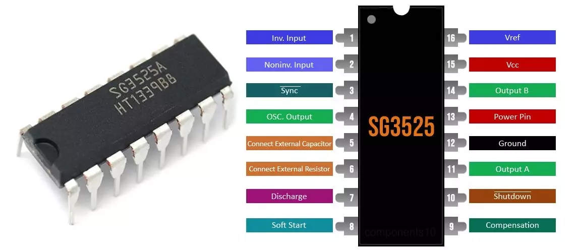
- Pin 1 (INV): Inverting input of the error amplifier, used for feedback from the output.
- Pin 2 (NI): Non-inverting input of the error amplifier, often tied to a reference voltage.
- Pin 3 (SYNC): Synchronization pin, allows for synchronization with an external clock.
- Pin 4 (OSC): Connects to the timing capacitor for controlling oscillator frequency.
- Pin 5 (CT): Timing capacitor pin, defines the frequency of the internal oscillator.
- Pin 6 (RT): Timing resistor pin, which also helps in setting the oscillator frequency.
- Pin 7 (DISCHARGE): Used to discharge the timing capacitor during each oscillator cycle.
- Pin 8 (SOFT-START): Controls the soft-start function by charging a capacitor to gradually increase output.
- Pin 9 (COMP): Provides compensation for loop stability in feedback circuits.
- Pin 10 (SHUTDOWN): A shutdown terminal that disables the output stages immediately when activated.
- Pin 11, 14 (OUT A, OUT B): Outputs for driving the external MOSFETs or transistors in the power stage.
- Pin 12 (VCC): The main supply voltage input for the IC.
- Pin 13 (GND): Ground pin.
- Pin 15 (VC): The output stage supply pin.
- Pin 16 (VREF): Provides a 5V reference voltage for external components.
The IC uses an under-voltage lockout feature to prevent operation when the input voltage is too low, ensuring stable performance. It also incorporates a soft-start functionality for controlled startup and protection mechanisms for safe operation in power systems.
SG3525 PWM Frequency Formula:
F = 1 / (CT × (0.7 RT + 3 RD))
Where:
- F = Frequency (Hz)
- CT = Timing Capacitor at pin 5 (F)
- RT = Timing Resistor at pin 6 (Ω)
- RD = Deadtime Resistor between pins 5 & 7 (Ω)
Suppose we have the following component values:
- CT = 1µF
- RT = 14kΩ
- RD = 47Ω
Substituting above values in the formula,
F = 1 / (1 × 10−6 × (0.7 × 14 × 103 + 3 × 47))
F ≈ 100.59 Hz
Power MOSFET Stage:
-
- The PWM outputs from the SG3525A are connected to the gates of the MOSFETs. The MOSFETs switch the DC power supply (e.g., 12V from a battery) on and off at a high frequency.
- The MOSFETs are connected to the primary winding of a center-tapped transformer. The center tap is connected to the positive terminal of the battery, while the two ends of the primary winding are connected to the drain terminals of the MOSFETs.
- The secondary winding of step-up transformer produces an AC voltage to the desired level (e.g., 110V or 220V AC).
Filter and Load:
-
- The AC output from the transformer can be filtered using inductors and capacitors to remove high-frequency noise.
- The filtered AC output can be used to power AC loads.
3. Key Considerations:
- Frequency: The oscillator frequency (set by RT and CT) typically ranges from 100Hz to 100kHz, depending on the application.
- Heat Dissipation: Ensure proper heat sinking for MOSFETs to manage heat dissipation.
- Feedback Loop: If voltage regulation is needed, design a feedback loop to maintain a stable output voltage.
- Safety: Include protection mechanisms like fuses, diodes, and capacitors to prevent damage from over-voltage, over-current, or reverse polarity.
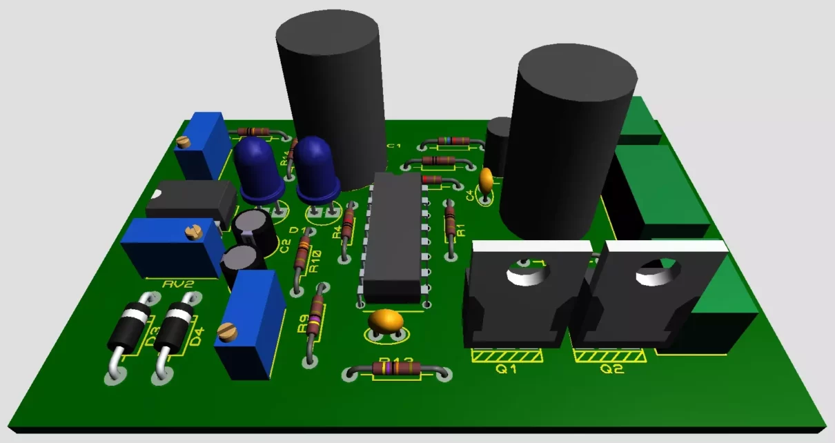
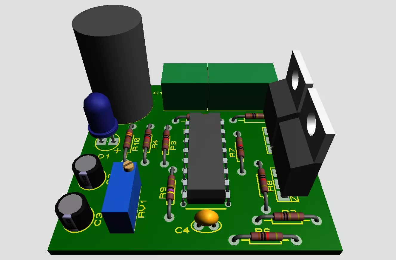
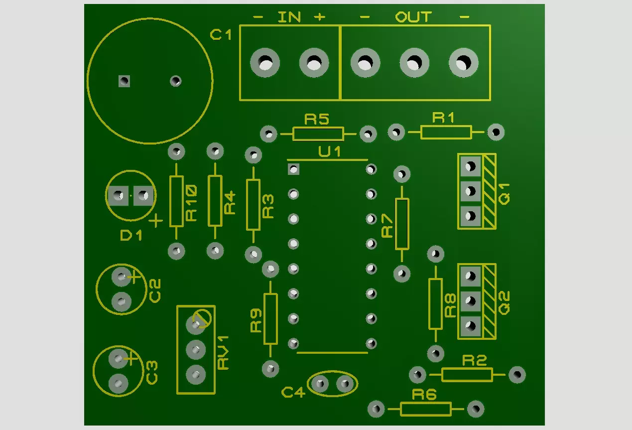
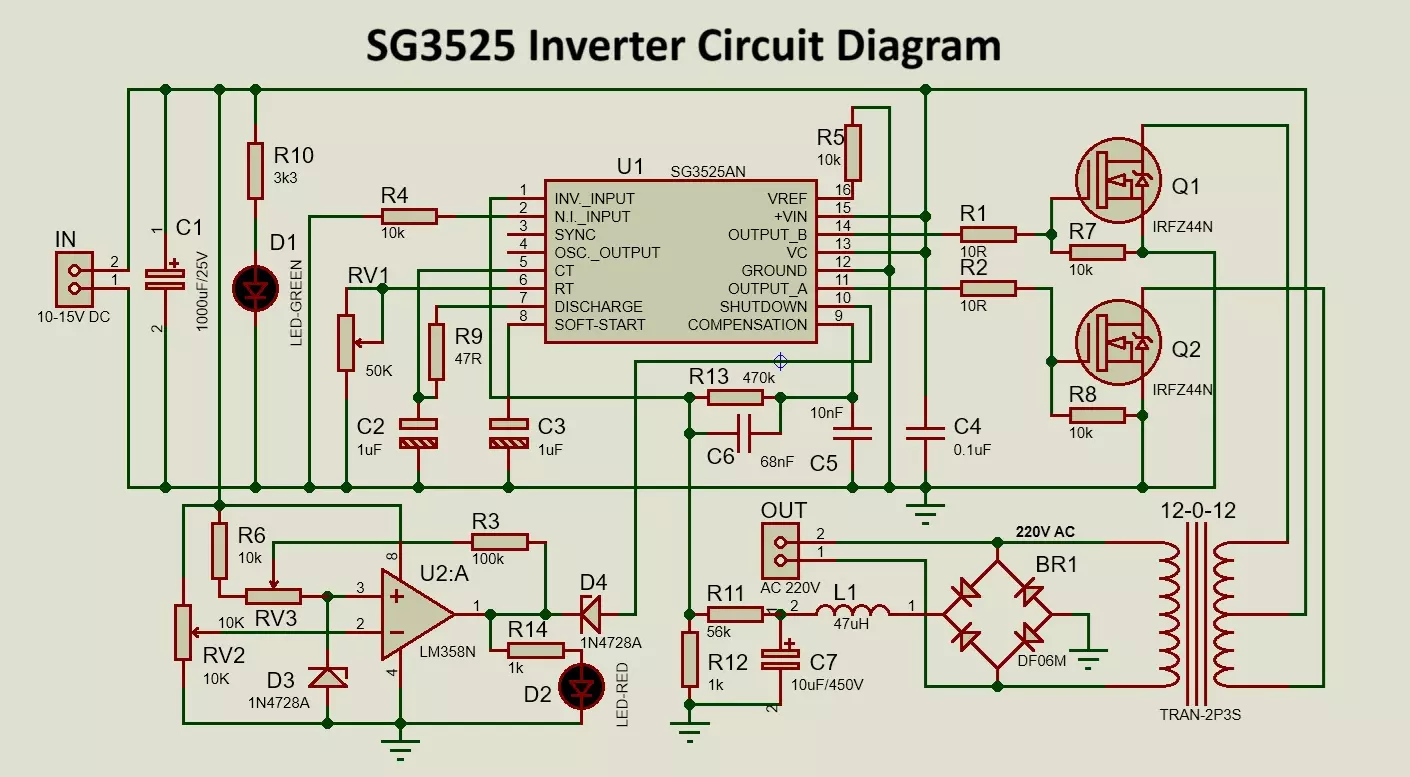
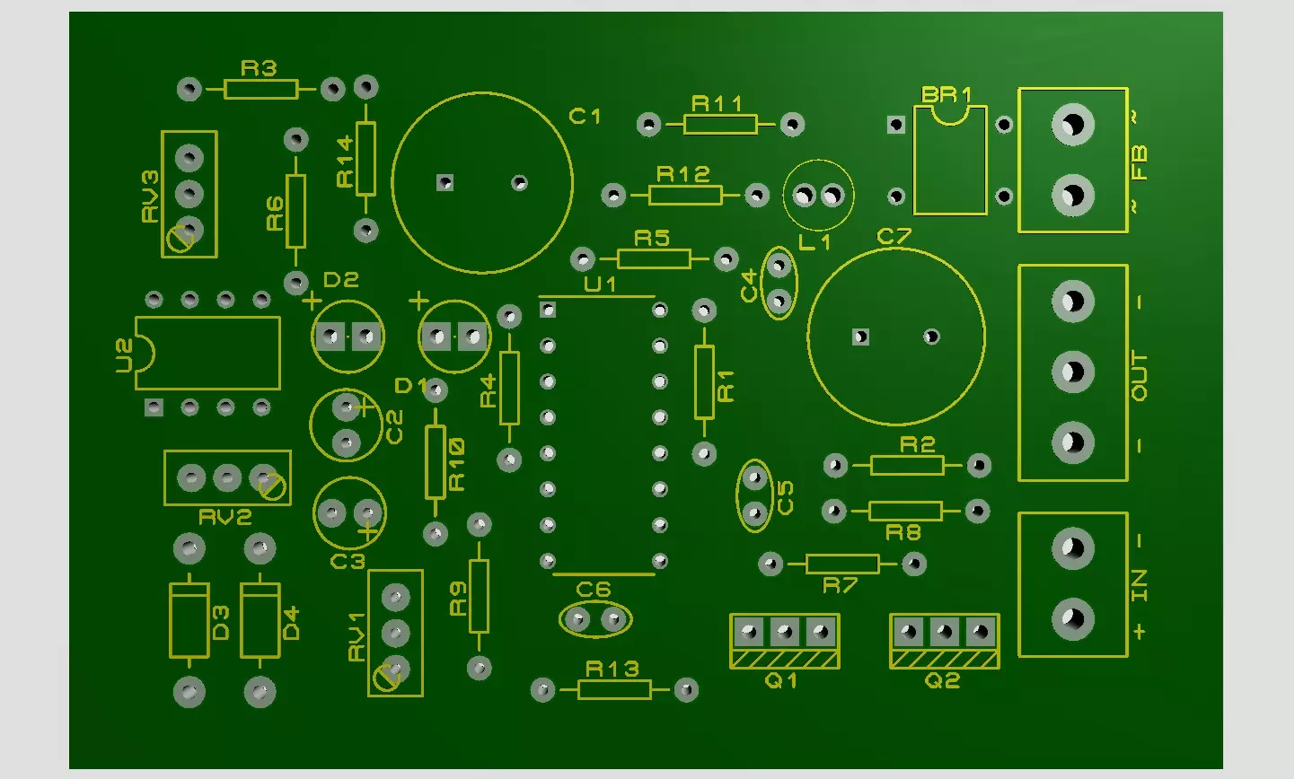
Basic SG3525 Inverter Circuit Diagram:
The circuit diagram below shows the basic Inverter by SG3525A IC. The output pins (11 and 14) drive the gates of the MOSFETs, which, in turn, drive the transformer to convert DC to AC. 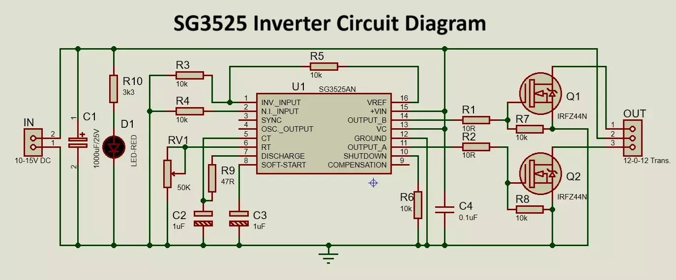
Components List:
- R1, R2 = 10Ω
- R3, R4, R5, R6, R7, R8 = 10kΩ
- R9 = 47Ω
- R10 = 3.3kΩ
- RV1 = 50kΩ preset
- C4 = 0.1uF
- C2, C3 = 1uF
- C1 = 1000uF/25V
- D1 = Red LED
- Q1, Q2 = IRFZ44N MOSFETs
- U1 = SG3525A IC
- 12-0-12 Transformer
- 12V Battery
- 2,3 Screw terminals
Here is a video demonstrating this Simple SG3525 Inverter Circuit.
This is a simplified inverter circuit using the SG3525A. Depending on the specific application, additional components and considerations may be necessary for efficiency, stability, and safety. Here is how it will look like after fully assembled on PCB,
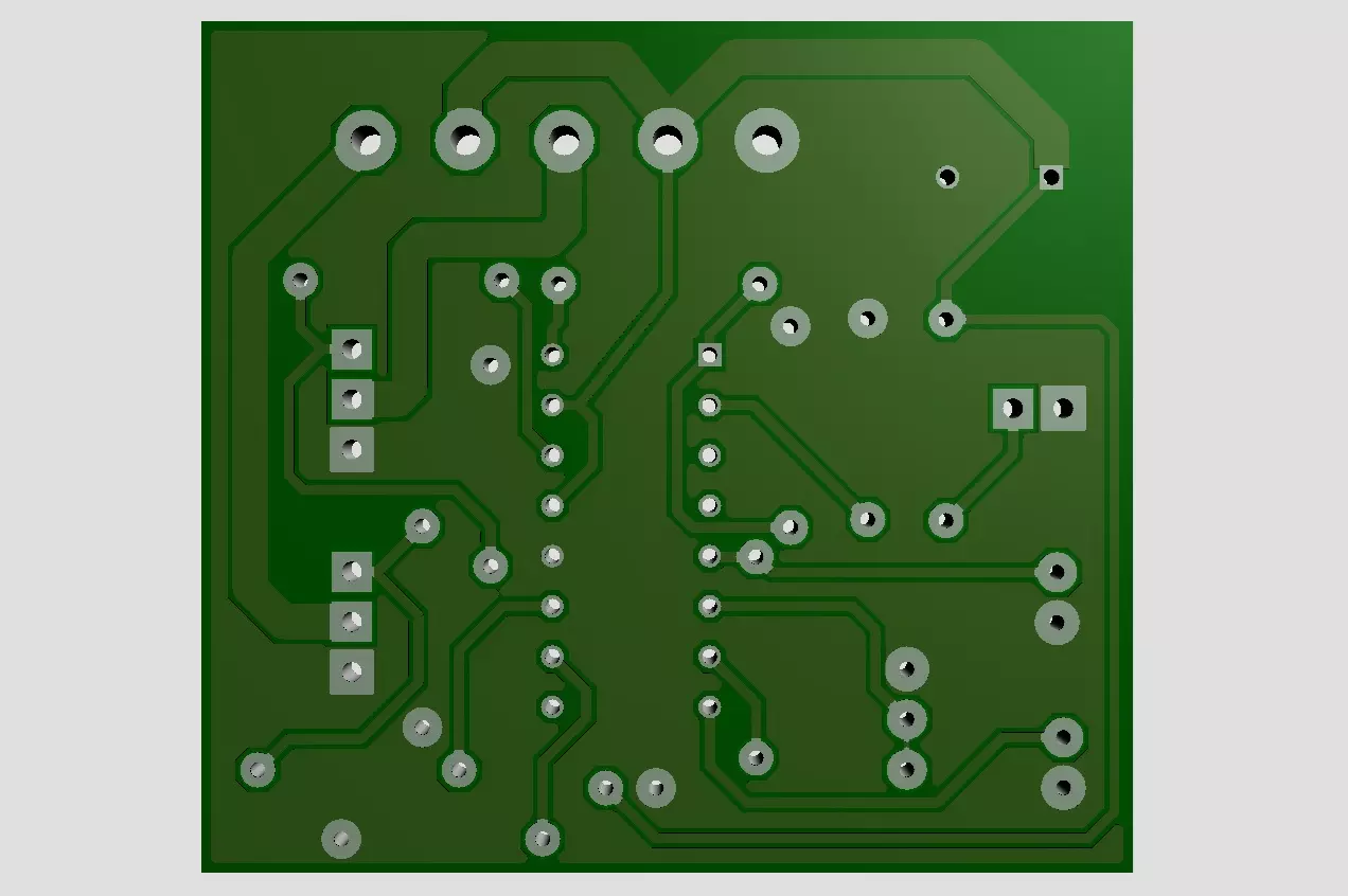
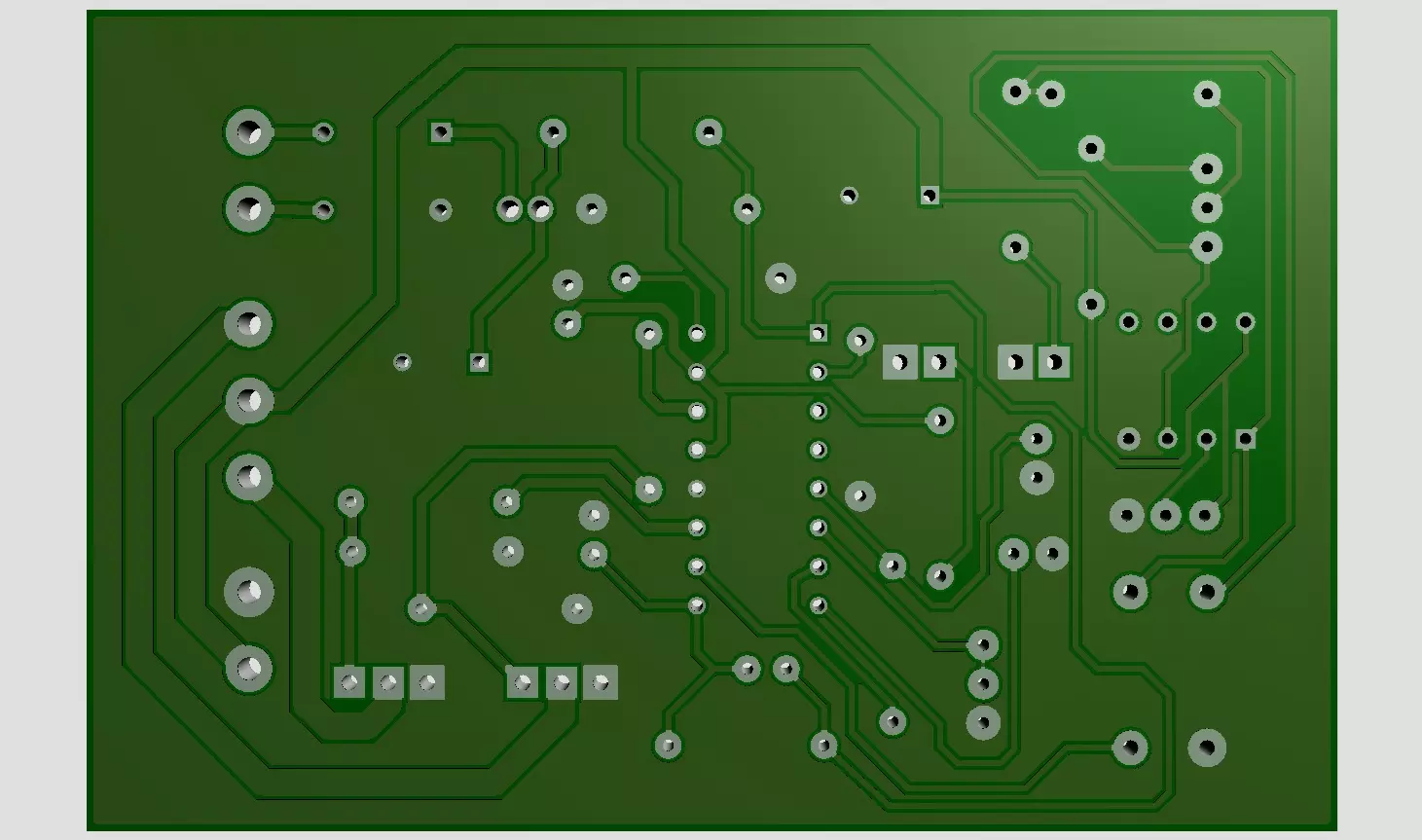
Here are the top and bottom images of PCB without component.
- Connect a 12V lead acid or Li-Po battery to input terminal (IN) + & -.
- A step-up transformer is required to convert low-voltage DC (typically 12V or 24V from the battery) to the required AC voltage (typically 220V or 110V). The transformer should have the correct turns ratio to ensure proper output voltage.
- Connect 12-0-12 terminal of transformer to output terminals (OUT) 1, 2 and 3.
You can clearly see that for high current section PCB copper traces have been made thick.
Download the above SG3525 inverter circuit files from here,
SG3525 Inverter Circuit with Output Voltage regulation and Low Battery Cut-Off:
To design SG3525 based inverter circuit with output voltage regulation and low battery cut-off using the SG3525, you will need a combination of additional components for feedback, voltage sensing, and low battery monitoring.

Key Components:
Here’s an overview of the circuit elements:
- SG3525 IC: The heart of the circuit that generates PWM signals for switching MOSFETs.
- Driver Circuit: To interface the SG3525A with the big MOSFETs/IGBTs.
- MOSFETs: Power switching transistors (commonly N-channel MOSFETs like IRF3205) to drive the transformer.
- Transformer: Step-up transformer to convert low-voltage DC to higher voltage AC.
- Voltage Feedback Circuit: To regulate the output voltage.
- Low Battery Cut-off Circuit: To disconnect the load when the battery voltage drops below a safe threshold.
- Protection Circuits: To avoid overcurrent and short-circuit situations. (optional)
- Low-pass Filter: To filter the PWM output into a sine wave. (optional)
SG3525 Inverter Circuit Schematic:
Components List:
- R1, R2 = 10Ω
- R3 = 100kΩ
- R4, R5, R6, R7, R8 = 10kΩ
- R9 = 47Ω
- R10 = 3.3kΩ
- R11 = 56KΩ
- R12, R14 = 1kΩ
- R13 = 470kΩ
- RV1 = 50kΩ preset
- RV2, RV3 = 10kΩ preset
- L1 = 47uH inductor
- C4 = 0.1uF
- C2, C3 = 1uF
- C1 = 1000uF/25V
- C5 = 10nF
- C6 = 68nF
- C7 = 10uF/450V
- D1 = Green LED
- D2 = Red LED
- D3, D4 = 1N4728A Zener
- Q1, Q2 = IRFZ44N MOSFETs
- U1 = SG3525A IC
- 12-0-12 Transformer
- 12V Battery
- 2,2,3 Screw terminals
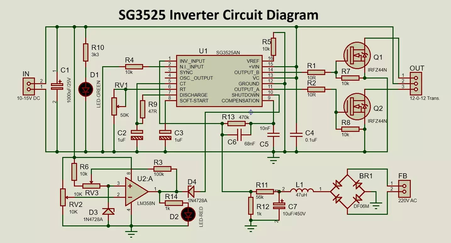
1. SG3525 PWM Controller:
- Pin 1 (INV) and Pin 2 (NI): These are used for feedback control to maintain regulated output voltage. A resistive divider from the output (after the transformer) will provide a feedback signal to the SG3525 to adjust the PWM duty cycle accordingly.
- Pin 5 (Oscillator Timing Capacitor): Used to set the frequency of the internal oscillator, which determines the switching frequency of the MOSFETs (typically 50 Hz for AC output).
- Pin 6 (Oscillator Timing Resistor): Sets the timing for the internal oscillator in conjunction with the capacitor on Pin 4.
- Pin 7 (DISCHARGE): Used to discharge the timing capacitor during each oscillator cycle.
- Pin 8 (Soft Start): A capacitor is placed here to control the ramp-up time of the PWM signal. This prevents high inrush current.
- Pin 9 (COMP): Provides compensation for loop stability in feedback circuits.
- Pin 10 (SHUTDOWN): A shutdown terminal that disables the output stages immediately when low battery is detected by OPAMP circuit.
- Pin 11 and 14 (Output A & B): These are the complementary PWM outputs used to drive the MOSFETs.
2. MOSFET Power Stage:
The PWM signals from the SG3525 will drive the gates of N-channel MOSFETs (IRFZ44N). These MOSFETs are responsible for switching the DC voltage from the battery across the primary of the transformer. A typical H-bridge configuration or push-pull setup is common in such designs.
- Gate Resistors: To control the gate drive of the MOSFETs and prevent gate ringing.
- Flyback Diodes: Across the MOSFETs to protect against voltage spikes due to transformer inductance.
3. Transformer:
- A step-up transformer is required to convert low-voltage DC (typically 12V or 24V from the battery) to the required AC voltage (typically 220V or 110V). The transformer should have the correct turns ratio to ensure proper output voltage.
- Connect a 12V lead acid or Li-Po battery to input terminal (IN) + & -.
- Connect 12-0-12 terminal of transformer to output terminals (OUT) 1, 2 and 3.
Thick PCB tracks can handle more current use solder to make it even better.
4. Output Voltage Regulation:
- A voltage divider network from the output of the transformer (AC side) is used to sense the output voltage. This divided voltage is fed back to the SG3525’s error amplifier (Pin 1).
- Connect transformer output to feedback input terminal (FB).
5. Low Battery Cut-Off:
To protect the battery from over-discharge, a low battery cut-off circuit is necessary. This can be implemented using a comparator circuit or a low-voltage sensing IC like LM393 or LM358, which monitors the battery voltage. When the voltage falls below a preset threshold (e.g., 10.5V for a 12V system), the cut-off circuit will disable the SG3525’s output or it can disconnect the load.
- Voltage Divider for Battery Monitoring: A voltage divider reduces the battery voltage to a suitable level for the comparator or sensing circuit.
- The Zener diode provide voltage reference and protects pin 10 of 3525 IC.
- Comparator: When the battery voltage falls below the reference set by the divider, the comparator will output a signal that will disable the SG3525 (e.g., by pulling the shutdown pin low or via a relay).
Considerations:
- Feedback Control: Proper feedback is required for voltage regulation and to maintain a stable output frequency.
- Heat Management: Ensure proper heat sinks are used for the MOSFETs/IGBTs to manage heat dissipation.
- Overcurrent Protection: Implement protection circuits to prevent damage to components in case of short circuits or overloads.
- Low-Pass Filter: Use an LC filter (Inductor-Capacitor) to smooth the transformer output into a sine wave.
Download the above SG3525 PWM inverter circuit files from here,
Conclusion:
The SG3525 inverter circuit offers a versatile and efficient solution for generating both modified and pure sine wave AC outputs. It operates using a basic PWM technique to regulate the output voltage, making it suitable for powering various electronic devices. With simple modifications, such as adding an SPWM generator, the circuit can produce a pure sine wave output, improving its performance for sensitive appliances. Additionally, features like low battery protection and automatic voltage regulation make the SG3525 inverter a reliable choice for both basic and advanced inverter applications.
3 Simple IR Proximity Sensor Circuits with Working & Applications
Star Delta Connection in Three Phase Power Systems

Nice!!!
Thanks be to Lord Jesus!!!
we need to make invertor man made when i finish transisto it brasting can help me that it can stop that
What are you trying to say? make it clear!
Hi, thanks for the good work and sharing the knowledge. Is it possible to have over-current protection integrated with the low battery protection? If yes can you upload such circuit. Cheers
Ok I will work on it.
Nice article , very informative . Thank you
Is it possible to get a full H-Bridge version of the above circuits, please?
Here is the H bridge version of above circuit
https://www.hackatronic.com/h-bridge-inverter-circuit-using-ic-sg3525-and-mosfet-irfz44n/
Few questions please! What is the purpose of connecting pin 16 Vref to ground through a 10K resistor? What is the purpose of connecting pin 2 non-inverting input to ground through a 10K resistor? Most examples I see connect pin 2 and 16 together through a 1K resistor, but I’m having a problem with the oscillator starting like that.
– On pin 16, a 10K resistor to ground lightly loads the reference output. This helps maintain the proper 5V level without drawing excessive current.
– On pin 2, a 10K resistor to ground sets a gentle bias for the error amplifier’s non-inverting input. This lower loading (compared to a 1K resistor or a direct tie to 5V) avoids over-driving the input and permits the internal oscillator to begin its operation.
Hello, could you send me the proteus library of SG3525 ? My e-mail is [email protected], thanks !
You can find it in proteus
Hello, is this a modified square wave inverter circuit.
It’s a square wave inverter.
There is no SG3525 on Proteus…
Search it properly!
Timing Oscillator Capacitor. If pin 5 is meant for TOC, why is is it not connected to one or how are we producing the 50Hz pwm/SPWM signal?
You are talking about which circuit?
Please I tried this circuit but I had to connect pin 10 to ground before it worked which I thought shouldn’t be. I need your help please.
You can see in the circuit pin 10(shutdown) is connected to ground via 10k resistor R6.
I highly appreciate your prompt response sir , thanks you very much. I was referring to your inverter circuit that has LM 358 circuit connected pin10 of sg3525 without seeing the pin 10 being connected to ground via 10k resistor. Again should reset the LM 358 before connecting it? I count on your usual response.
This circuit is having problem, if you are using LM358 then tell me how was the performance and behavior of this circuit?
Thanks, the circuit works well only when I connect pin 10 to ground without 10k resistor. The LED on lm358 battery low circuit glows when adjusted using the 10k preset on LM 358 pin 2, but the 10k preset on pin 3 gives no control when adjusted
You can see there is a Zener diode D3 1N4728A which keeps voltage at pin 3 at 3.3V.
The 10k Preset is here to adjust the current, also it’s a part of feedback.
Can you see if there is any effect on circuit in the absence of this feedback path?
Is that low battery auto-cut-off circuit working properly?
Thanks you so much, I will verify.
Sir, I checked the LM 358 low battery cut off. When l set set the cut off at 10 volts, and I use 9 volt for the inverter it doesn’t cut off but still operates. In this circuit diagram having the low battery cut off , you connected pin 10 direct to the LM 358 and I also did the same. I need your guidance on this please, and also can replace the DF06M bridge rectifier with IN5408 diodes bridge rectifier?
You can replace the DF06M bridge rectifier with IN5408 diodes bridge rectifier.
For cut off try checking at some lower voltage, LM358 can operate from a single supply, but its input common mode range is from 0V to Vcc-1.5V
Check this comparator section separately whether it is working properly or not.
Also, you can use LM393 comparator for implementing this circuit.
Thanks you Sir, I will verify.
Please can I use lm 7805 for the input voltage for the inverter
No, it’s not a 5V IC
How are you sir, please I made your circuit having the battery low cut off and it was working properly. When I tried to add overload protection circuit, the IC burned. I changed replaced the IC and other companies but It isn’t working.
Could you please show me your overload protection circuit.
You can contact me via email or WhatsApp.