Energy band theory of solids explains why some solids conduct electricity easily, why some do not, and why others behave in-between. Classical physics could not explain electrical conduction fully, but quantum mechanics and band theory together provide a complete picture.
Solids are materials in which atoms are closely packed in a regular or irregular arrangement. In crystalline solids, atoms form a periodic and orderly lattice, while in amorphous solids, the arrangement is random. Each atom contains electrons revolving around the nucleus in discrete, quantized energy levels.
When atoms are isolated, these energy levels are well-defined and separated by significant energy differences. However, in solids, millions of atoms come together, and their electron clouds overlap. As a result, individual energy levels split into a very large number of closely spaced levels, forming energy bands.
Formation of Energy Bands
1. Overlapping of Atomic Orbitals
When atoms are brought close to form a crystal lattice, their outermost electron orbitals overlap. Due to the Pauli Exclusion Principle, no two electrons can occupy the same quantum state. Thus, each atomic energy level must split into many slightly different levels to accommodate electrons from each atom.
2. Splitting and Formation of Bands
As the number of interacting atoms increases (typically ~10²³ atoms in a solid), the split levels become so closely spaced that they appear continuous. These continuous regions are called energy bands.
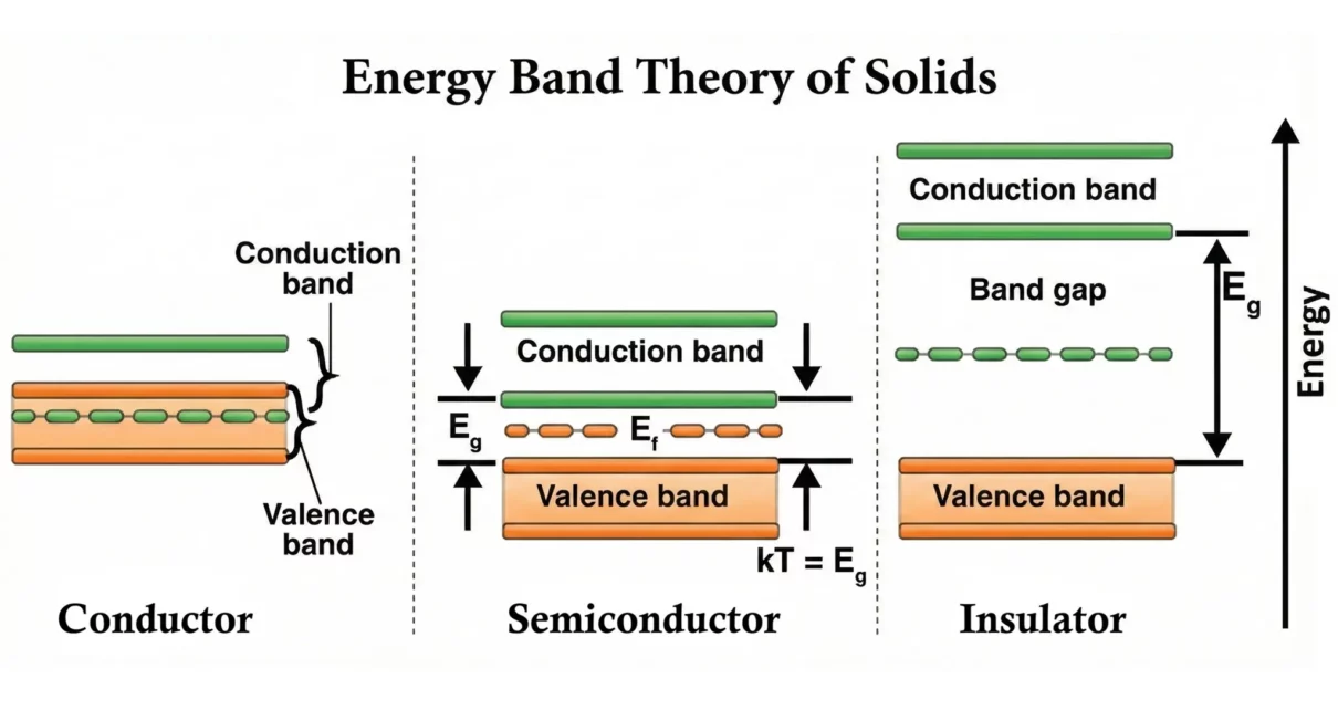
Two most important bands are:
1. Valence Band (VB)
- Formed by electrons involved in bonding.
- Usually, the highest fully or partially occupied band at 0 K.
- Determines how tightly electrons are bound to atoms.
2. Conduction Band (CB)
- Higher energy band where electrons are free to move.
- Electrons in this band behave like free charge carriers.
Band Gap / Forbidden Energy Gap (Eg)
Between the valence band and conduction band lies a region where no allowed electron states exist. This forbidden region is called the band gap.
- Small gap → easier for electrons to jump to conduction band
- Large gap → nearly impossible at normal temperatures
Fermi Level (EF)
The Fermi level is the energy level at which the probability of finding an electron is 50% at thermal equilibrium (0 K definition).
Its position relative to VB and CB determines a material’s electrical behavior.
Classification of Solids Based on Band Structure
The electronic properties of solids depend strongly on how the energy levels of electrons are arranged. When atoms come together to form a solid, their discrete atomic orbitals split into bands of energy levels. Based on them, solids are broadly classified into:
- Conductors
- Insulators
- Semiconductors
The classification depends primarily on:
- Size of the band gap (Eg)
- Position of the Fermi level (EF)
- Number of free charge carriers (electrons or holes)
Conductors
Conductors allow electrons to move freely, which results in high electrical conductivity.
Band Structure of Conductors
There are two main scenarios that allow easy conduction:
1. Overlapping Valence and Conduction Bands
- The valence band merges with the conduction band.
- No forbidden energy gap exists.
- Electrons naturally have available empty states to move into.
2. Partially Filled Conduction Band
- Even if the bands do not overlap, the conduction band is not fully filled.
- Electrons can move easily because empty energy levels are already available.
Key Characteristics
- Band gap Eg ≈ 0 eV (none or extremely small)
- Very high electrical and thermal conductivity (due to lots of free electrons)
- Free electrons are present even at room temperature
- Conductivity decreases slightly as temperature increases
→ More heat → more lattice vibrations → more electron scattering.
Examples: Copper (Cu), Silver (Ag), Aluminum (Al), Iron (Fe) and most metals.
Insulators
Insulators resist the flow of electric current because electrons cannot move freely.
Band Structure of Insulators
- Valence Band: Completely filled
- Conduction Band: Completely empty
- Large band gap (Eg > 3 eV)
The gap is so large that:
- Electrons cannot jump from VB to CB with normal thermal energy.
- Very few charge carriers are available.
Properties
- Very low electrical conductivity
- Even at high temperatures, only a negligible number of electrons reach the conduction band
- Conductivity increases only at extremely high temperatures, but still remains low
Examples: Glass, Plastic, Rubber, Wood, Mica, Ceramics.
Semiconductors
Semiconductors have properties between conductors and insulators.
Band Structure of Semiconductors
- Moderate band gap: typically, 0.7 – 1.5 eV
- Much smaller than insulators
- At room temperature, some electrons gain enough thermal energy to cross the band gap
→ Small but significant number of electrons enter the conduction band
Conductivity Properties
- Poor conductors at low temperature (few charge carriers)
- Conductivity increases with temperature
- More electrons excited from VB to CB
- Conductivity can be greatly enhanced by doping
- Adding impurities creates extra electrons (n-type)
- Or creates holes (p-type)
This tunability is what makes semiconductors extremely important in electronics.
Examples: Silicon (Si), Germanium (Ge), Gallium arsenide (GaAs), Indium phosphide (InP).
Types of Semiconductors
- Intrinsic (pure) semiconductors
- Extrinsic (doped) semiconductors
Fermi Level
- Lies near the middle of the band gap
- Moves toward conduction or valence band depending on doping
Common Semiconductor Materials
- Silicon (Si) — Eg ≈ 1.12 eV
- Germanium (Ge) — Eg ≈ 0.66 eV
- Gallium arsenide (GaAs) — Eg ≈ 1.42 eV
Intrinsic Semiconductors
Intrinsic semiconductors are pure with no impurity atoms.
Examples: Pure Silicon, Pure Germanium.
Characteristics
- At 0 K → behave like insulators
- At room temperature → some bonds break → free electrons + holes
Electron-Hole Pairs
When an electron jumps to the conduction band:
- A free electron is created
- A hole (positive charge carrier) is left behind
Electron and hole concentrations are equal: n = p = ni
Fermi Level: Located approximately at the center of the band gap.
Extrinsic Semiconductors
Doping is the process of adding small amounts of impurity atoms to intrinsic semiconductors to improve their conductivity.
A. n-Type Semiconductors
Impurity type: Donor atoms (pentavalent: P, As, Sb)
How They Work?
- Donor atoms have 5 valence electrons
- 4 electrons form covalent bonds
- The 5th electron becomes a free conduction electron
- Electrons are the majority carriers
- Holes are minority carriers
Fermi Level: Moves closer to the conduction band.
B. p-Type Semiconductors
Impurity type: Acceptor atoms (trivalent: B, Al, Ga, In)
How They Work?
- Acceptor atoms have only 3 valence electrons
- Create a “hole” in the crystal
- Electrons from Si/Ge fill the hole → hole moves
- Holes are the majority carriers
- Electrons are minority carriers
Fermi Level: Moves closer to the valence band.
Comparison: Conductor vs Semiconductor vs Insulator
Here is a comparison table of conductors, semiconductors and insulators according to energy band theory.
| Property | Conductors | Semiconductors | Insulators |
|---|---|---|---|
| Band Gap (Eg) | ~0 eV | ~1 eV | > 3 eV |
| VB-CB Overlap | Yes/partial | No | No |
| Fermi Level | Lies within partially filled band | Middle / shifts with doping | Deep within gap |
| Temperature Effect | Conductivity ↓ with T | Conductivity ↑ with T | Almost no change |
| Charge Carriers | Many free electrons | Few e–h pairs | Almost none |
| Conductivity | Very high | Moderate | Very low |
Applications
Conductors
- Electrical wiring:
Copper and aluminum wires in homes, industries, and power transmission. - Power transmission lines:
High-voltage cables made of aluminum and steel. - Electrical components:
Used in switches, connectors, plugs, and sockets. - Metallic casings:
Used in devices where grounding is needed (e.g., metal bodies of appliances). - Printed circuit boards (PCBs):
Copper tracks connect electronic components.
Semiconductors
- Diodes and LEDs:
Used for rectification, lighting, and displays. - Transistors:
Used as switches or amplifiers in all electronic devices. - Integrated circuits (ICs) / Microchips:
Used in computers, smartphones, calculators, etc. - Solar cells (photovoltaics):
Silicon converts sunlight into electricity. - Sensors:
Temperature sensors, photodetectors, gas sensors. - Microcontrollers and microprocessors:
Found in nearly all modern electronic systems (cars, appliances, robotics).
Insulators
- Electrical insulation:
Rubber, PVC, or plastic covering on wires. - Support in power systems:
Ceramic insulators on electric poles. - Protective casings:
Plastic bodies of appliances to prevent electric shock. - Capacitors (dielectric material):
Mica, ceramic, plastic films. - Insulating bases:
Used in circuit boards and switchgear. - High-voltage equipment:
Glass and porcelain insulators used in transmission lines.
Q&A on Energy Band Theory of Solids
1. What do energy band diagrams show?
Energy band diagrams display the relative positions of the Valence Band (VB), Conduction Band (CB), Band Gap (Eg), and the Fermi Level (EF) for conductors, semiconductors, and insulators.
2. Why do conductors have free electrons?
Because in conductors, the valence band and conduction band overlap, allowing electrons to move freely without needing extra energy.
3. Why do semiconductors need thermal energy for conduction?
Semiconductors have a small band gap, so electrons require thermal energy (or light) to jump from the valence band to the conduction band.
4. Why do insulators resist conduction?
Insulators have a very large band gap. Electrons cannot cross this gap under normal conditions, resulting in very low conduction.
5. What does the conductivity vs temperature graph show for different materials?
- Semiconductors: Conductivity increases exponentially with temperature.
- Conductors: Conductivity decreases slightly with temperature due to increased resistance.
- Insulators: Conductivity remains almost constant and very low.
6. What is the formula for intrinsic carrier concentration ni?
ni = A T3/2 e-Eg / (2 k T)
Where:
- ni = intrinsic carrier concentration
- A = material constant
- T = temperature
- Eg = band gap energy
- k = Boltzmann constant
7. What does this formula indicate about semiconductor behavior?
Even a small increase in temperature produces a large increase in carrier concentration because of the exponential dependence. This explains the rapid rise in semiconductor conductivity with temperature.
8. What is drift velocity?
Drift velocity vd is the average velocity of charge carriers when an electric field is applied.
9. What is mobility?
Mobility µ describes how easily charge carriers move through a material under an electric field.
10. What is the relation between drift velocity and electric field?
vd = µE
11. What is the difference between direct and indirect band gap semiconductors?
- Direct band gap: Electrons recombine with holes directly and emit photons. Used in LEDs, lasers, GaAs.
- Indirect band gap: Recombination requires phonons, so photon emission is weak. Silicon (Si) is the main example.
12. What is effective mass?
Effective mass describes how electrons behave as if they have a modified mass due to the curvature of the energy band. Flatter bands mean heavier effective mass; steeper bands mean lighter effective mass.
13. What is the Fermi-Dirac distribution?
It gives the probability that an energy state is occupied by an electron:
f(E) = 1 / (1 + e(E - EF)/(kT))
14. How do crystalline solids differ from amorphous solids in terms of band structure?
- Crystalline solids: Well-defined, sharp energy bands due to ordered atomic arrangement.
- Amorphous solids: Broadened bands and localized states due to structural disorder.
15. What are superconductors and how does band theory explain them?
Superconductors exhibit zero electrical resistance below a critical temperature. Band theory is extended to include Cooper pairs, where electrons pair up and move without scattering.
Summary
Energy band theory is fundamental for explaining electrical behavior in solids.
It reveals that:
- Conductors have overlapping or partially filled bands → high conductivity
- Insulators have a large band gap → no free electrons
- Semiconductors have a moderate band gap → conductivity can be controlled
This simple concept of band gap is the backbone of modern electronics.
Semiconductors, engineered through doping and material design, power everything from mobile phones to solar panels, computers, power devices, and communication systems.
Therefore, understanding energy band theory of solids is crucial for physics, electrical engineering, electronics, and material science.
Laser Diode – Symbol, Construction, Working, Types and Applications
Light Emitting Diode LED – Symbol, Construction, Working, Types and Applications
Photodiode – Symbol, Construction, Working, Types and Applications
Phototransistor – Construction, Working, Types and Applications
