This article explains clamper circuits from the ground up including their types, mathematical analysis, waveforms, working principle, differences, applications, and real-world design considerations.
Clamper circuits are fundamental waveform-shaping networks used in electronics to shift the entire signal level either upward or downward without altering the overall shape of the waveform. Unlike clippers, which remove or “clip” a portion of the waveform, clampers add a DC level to the input AC signal. This makes them essential in oscilloscopes, communication systems, detectors, and analog interfacing circuits.
Introduction to Clamper Circuits
What is a Clamper Circuit?
A clamper circuit (also called a DC restorer or level shifter) is an electronic circuit that shifts an AC signal to a different DC level without changing the peak-to-peak amplitude.
What a Clamper Does?
A clamper adds or subtracts a DC component to an AC input signal.
- If the DC level is added, the waveform shifts upward.
- If the DC level is subtracted, the waveform shifts downward.
The essential idea is that the waveform is “clamped” to a new reference level (not necessarily 0 V).
Why is a Clamper Needed?
Many electronic systems require a signal to be placed above or below a reference level:
- To display AC signals on an oscilloscope with desired alignment.
- To convert bipolar signals into unipolar voltages for ADC input.
- To restore DC components removed during AC coupling in communication systems.
How a Clamper Circuit Works?
The operation relies on the combined behavior of the diode, capacitor, and resistor:
- Capacitor Charging Phase
During one half-cycle of the input AC signal, the diode becomes forward biased and allows current to flow.- The capacitor charges to (approximately) the peak input voltage during this period.
- Capacitor Discharging / DC Addition Phase
During the opposite half-cycle, the diode becomes reverse-biased and stops conducting.- The capacitor now acts as a voltage source, adding its stored charge to the input signal.
- Because of this, the entire signal shifts up or down by the capacitor’s voltage.
RC Time Constant Requirement
To maintain proper clamping:
RC >> T = 1/f
Where:
- R = load resistance
- C = capacitor
- T = time period of the signal
- f = signal frequency
This ensures the capacitor does not discharge significantly and holds a stable DC voltage.
As long as the RC time constant is large enough (ensuring the capacitor does not discharge significantly during a cycle), the waveform shape remains intact—only its vertical position changes.
Key Points
- A clamper does not distort the waveform.
- It shifts the signal relative to the reference (usually 0 V).
- It uses the capacitor’s stored charge to create the DC shift.
- Clampers can be configured to shift the waveform positive or negative depending on diode orientation.
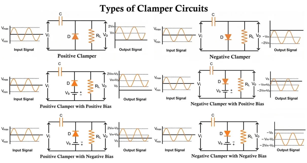
Types of Clamper Circuits
Clamper circuits are classified based on diode polarity and additional biasing.
- Positive Clamper
- Positive Clamper with Biasing (Positive / Negative bias)
- Negative Clamper
- Negative Clamper with Biasing (Positive / Negative bias)
Positive Clamper Circuit
A positive clamper shifts the entire input waveform upward, raising it above the 0 V reference line. The purpose of this circuit is to add a positive DC level to the AC signal so that all parts of the waveform appear in the positive region.

Operation of the Positive Clamper
A positive clamper works by:
- Charging the capacitor during the negative half cycle,
- Using the stored voltage to shift the signal upward during subsequent cycles,
- Producing an output waveform whose minimum value is raised above zero.
1. During the Positive Half Cycle
- The diode is reverse biased, so it does not conduct.
- The input signal appears at the output unchanged, and the capacitor remains uncharged during this interval.
- Because no clamping occurs in this half cycle, the output here is not considered part of the clamped behavior.
2. During the Negative Half Cycle
- The diode becomes forward biased and starts conducting.
- The capacitor charges up to the peak input voltage Vm, but with inverse polarity.
- By the end of this half cycle, the capacitor stores a voltage approximately equal to Vm.
3. Next Positive Half Cycle
- The diode is reverse biased again and remains off.
- The charged capacitor now acts like a voltage source in series with the input signal.
- Its stored voltage adds to the incoming AC voltage, causing the output to reach nearly 2Vm.
Vo ≈ Vm + Vm = 2Vm
As a result, the entire waveform is shifted upward, staying above the 0 V reference.
Positive Clamper Circuit with Biasing
A positive clamper can be modified by adding an external DC voltage source (biasing). This additional voltage shifts the waveform further upward or downward depending on the polarity of the bias.
- Positive biasing shifts the waveform upward by the bias voltage.
- Negative biasing shifts the waveform downward by the bias voltage.
This allows precise control of where the waveform sits relative to the reference (0 V) line.
Positive Clamper Circuit with Positive Biasing
In a positively biased positive clamper, a positive DC voltage source is added in series with the diode. This changes the capacitor’s charging level and therefore shifts the output waveform even higher.

Operation
- During the Positive Half Cycle
- The diode is reverse biased by the input signal but forward biased by the positive battery voltage.
- As a result, the diode conducts until the input voltage exceeds the battery voltage (Vb).
- During conduction, the capacitor charges approximately to (Vb).
- Once the input voltage rises above (Vb), the diode stops conducting.
- During the Negative Half Cycle
- The diode becomes forward biased by both the input voltage and the battery.
- The capacitor now charges to approximately:
Vc ≈ Vm + Vb
Next Positive Half Cycle
- The diode is reverse biased, and the capacitor does not discharge through it.
- The capacitor’s stored voltage adds to the input signal, shifting the entire waveform upward even more than a standard positive clamper.
Vshift ≈ Vm + Vb
Positive Clamper Circuit with Negative Biasing
A negatively biased positive clamper uses a negative voltage source in series with the diode. Although the diode and capacitor arrangement is the same, the negative bias voltage shifts the waveform downward by (Vb).

Operation
- During the Positive Half Cycle
- The diode is reverse biased by both the input voltage and the negative battery voltage.
- No conduction occurs, and the capacitor does not charge.
- During the Negative Half Cycle
- The diode becomes forward biased by the input signal but reverse biased by the battery voltage (Vb).
- The diode conducts only if the input voltage exceeds the magnitude of the battery voltage.
- When conduction occurs, the capacitor charges to approximately:
Vc ≈ Vm - Vb
This value is lower than in the unbiased clamper.
Next Positive Half Cycle
- The diode remains reverse biased.
- The capacitor adds its stored voltage to the input, shifting the waveform upward by:
Vshift ≈ Vm - Vb
Because a negative bias was used, the overall waveform is shifted downward by (Vb) compared to a standard positive clamper.
Negative Clamper Circuit
A negative clamper shifts the entire input waveform downward, moving it into the negative voltage region. The circuit operates similarly to a positive clamper but with the diode orientation reversed.

Operation of the Negative Clamper
A negative clamper works by:
- Charging the capacitor during the positive half cycle with reversed polarity,
- Adding this stored voltage to the incoming signal during the negative half cycle,
- Producing an output waveform shifted downward by approximately Vm, with peaks reaching as low as -2Vm.
- During the Positive Half Cycle
- The diode becomes forward biased, so it conducts.
- The capacitor charges to approximately the peak input voltage, but with inverse polarity (i.e., the capacitor charges to (-Vm)).
- Because the diode is conducting, the output during this interval is essentially zero and is not considered part of the clamped behavior.
- During the Negative Half Cycle
- The diode becomes reverse biased and stops conducting.
- The charged capacitor now acts as a voltage source in series with the input signal.
- Its stored voltage adds to the input waveform, producing an output that reaches approximately:
Vo ≈ -Vm + (-Vm) = -2Vm
This combined voltage shifts the entire waveform downward by the capacitor’s voltage.
Negative Clamper Circuit with Biasing
A negative clamper can be modified by adding a DC biasing voltage in series with the diode. Depending on the polarity of the bias:
- Positive biasing shifts the clamped waveform upward by the amount of the bias voltage.
- Negative biasing shifts the waveform further downward, increasing the negative offset.
Biasing therefore allows precise control over the vertical placement of the output waveform.
Negative Clamper Circuit with Positive Biasing
In a positively biased negative clamper, a positive DC voltage source (Vb) is placed in series with the diode. This reduces the charging level of the capacitor, resulting in an upward shift of the clamped waveform.

Operation
- During the Positive Half Cycle
- The diode is forward biased by the input signal but reverse biased by the positive battery voltage.
- The diode conducts only when the input voltage exceeds (Vb).
- As a result, the capacitor charges to a reduced level:
Vc ≈ - Vm + Vb
This is less negative than the capacitor voltage in an unbiased negative clamper.
- During the Negative Half Cycle
- The diode is reverse biased and does not conduct.
- The capacitor now discharges through the load, adding its voltage to the input waveform.
- The output waveform appears shifted upward by (Vb) compared to the standard negative clamper.
Thus, positive biasing raises the otherwise downward-shifted waveform.
Negative Clamper Circuit with Negative Biasing
In a negatively biased negative clamper, a negative DC voltage source is added in series with the diode. This increases the capacitor’s charging level, shifting the waveform even further downward.

Operation
- During the Positive Half Cycle
- The diode is forward biased by both the input signal and the negative battery voltage (since the battery assists the forward conduction).
- The diode conducts strongly, and the capacitor charges approximately to:
Vc ≈ - (Vm + Vb)
Since (Vb) is negative, this results in a more negative capacitor voltage than in the unbiased case.
- During the Negative Half Cycle
- The diode becomes reverse biased by the input signal, but the negative battery voltage may forward-bias it depending on the instantaneous input.
- When the input voltage exceeds the battery voltage in magnitude, the diode remains off.
- The output reflects the input plus the stored capacitor voltage, producing a deeper downward shift.
The waveform therefore moves further below zero, increasing the negative offset.
Mathematical Analysis of Waveforms
The waveform for a clamper circuit can be described as follows:
- The input AC signal oscillates symmetrically around 0 V.
- After clamping, the entire waveform is raised upward.
- The negative peak becomes 0 V.
- The positive peak becomes double the amplitude in ideal cases.
- Similarly, the negative clamper shifts the waveform downward, making the most positive peak approximately zero.
- Biased clampers shift the waveform by an adjustable amount, depending on the bias voltage and diode direction.
For an ideal positive clamper:
Vshift = Vm - Vd
- Vd = diode drop (0.7 V for Si, 0.3 V for Schottky)
- Vm = input peak voltage
If bias voltage Vb is added:
Vshift = Vm + Vb - Vd
In real circuits, a load resistor affects capacitor discharge.
- Small R → faster discharge → distortion
- Large R → stable clamping
Design Considerations for Clamper Circuits
Choosing Capacitor Value
A good practical rule:
C ≥ 10/2πfR
A larger capacitor provides better clamping with less ripple.
Diode Selection
- Use Schottky diodes for high-frequency applications.
- Use fast recovery diodes when working with pulse circuits.
Effect of Load Resistance
- Too small → capacitor discharges quickly → waveform distortion
- Too large → slow discharge → good clamping stability
Input Waveform Type
Clampers work well with:
- Sine waves
- Square waves
- Triangle waves
- Pulses
Pulse clampers are commonly used in digital logic interfacing.
Advantages of Clamper Circuits
- Simple and economical construction
Clamper circuits require only basic passive components, making them easy to design and cost-effective. - Preserves waveform shape
The circuit shifts the DC level of the signal without distorting the waveform under correct operating conditions. - Does not require an external power supply
The circuit creates the required DC shift through capacitor charging, reducing system complexity. - Useful for DC restoration
It restores the lost DC component of a signal in communication or display systems. - Effective for signal conditioning
Clampers are often used to level-shift signals for further processing in amplifiers or digital circuits.
Disadvantages of Clamper Circuits
- Performance depends on component values
Incorrect choice of capacitor or resistor can result in inaccurate clamping or waveform distortion. - Limited high-frequency operation
At high frequencies, the capacitor may not charge or discharge properly, reducing the effectiveness of the clamp. - Diode forward voltage drop affects accuracy
The clamping level is shifted by the diode’s forward voltage drop, causing deviation from the ideal value. - Sensitive to load variations
Changes in load resistance can affect the clamping voltage and overall performance. - Not suitable for precision applications without compensation
Variations in diode characteristics and frequency response make simple clamper circuits less precise.
Applications of Clamper Circuits
- DC restoration in television and display systems
Restores the lost DC component of video signals after AC coupling to maintain proper brightness and contrast. - Waveform shifting/positioning in oscilloscopes and measurement instruments
Shifts the entire waveform vertically so it fits within the display or measurement range. - Voltage multipliers in high-voltage power supplies
Acts in multiplier stages to shift voltage levels and store charge for generating high DC outputs. - Signal conditioning and level shifting for ADC inputs and sensors
Adjusts analog signal baselines to match ADC input limits and prevent clipping. - Pulse shaping and timing control in digital circuits
Shifts pulse baselines to establish correct timing and synchronization for digital logic. - Optical communication receivers (baseline restoration)
Restores the correct reference level of high-speed optical signals degraded by AC coupling. - Peak detection and envelope processing circuits
Shifts the waveform to a suitable DC level to accurately extract peaks or envelopes. - Intentional DC offset addition or removal (biased clampers)
Introduces or removes a predefined DC level to meet specific circuit requirements. - Voltage protection of electronic components
Limits excessive positive or negative voltage swings to protect sensitive device inputs. - Voltage level translation between circuits with different operating voltages
Shifts signal levels so circuits with different DC references can interface safely. - Reference level restoration in communication and transmission lines
Re-establishes the correct baseline of data signals after long-distance AC-coupled transmission. - RF and audio processing in AM/FM receivers
Shifts modulated signals to the required baseline for demodulation or amplification. - Biasing circuits to set amplifier operating points
Adds a fixed DC level to place signals within an amplifier’s linear region.
Summary
A clamper circuit is a simple yet powerful waveform processing tool that shifts an AC signal to a desired DC level without clipping.
- A clamper shifts an AC waveform’s DC level without clipping the peaks.
- The diode controls charge events; the capacitor stores the charge that provides the DC shift; a load resistor sets discharge rate.
- Positive and negative clampers move waveforms up or down; biasing lets you control the exact shift amount.
- Real-world performance is affected by diode drops, capacitor leakage/ESR, and load.
Using only a diode, capacitor, and resistor, clampers form the foundation of level shifting, DC restoration, pulse circuit and voltage multiplication techniques used in modern electronics.
Troubleshooting & FAQs
Q: Output not clamped to 0 V as expected.
A: Likely causes — diode forward drop, capacitor not large enough (RC too small), wrong diode polarity, heavy load (small R). Increase C, check diode orientation, use Schottky if diode drop is critical.
Q: Capacitor heating or failing (electrolytic case).
A: Electrolytics exposed to AC reversal will fail — use nonpolar film caps or ensure polarity never reverses.
Q: Waveform shows sag between peaks.
A: Sag indicates capacitor discharge through load — increase C or increase R (reduce load) so RC >> T.
Q: Why does a biased clamper sometimes not conduct in one half-cycle?
A: Because the bias shifts the conduction threshold. The diode may only conduct when the instantaneous input exceeds the bias level plus diode drop.
Q: Can I use a clamper for very low frequency signals (e.g., 1 Hz)?
A: In principle yes, but C must be huge to keep RC >> 1 s. This often becomes impractical; consider active level-shifters (op-amp circuits) instead.
Diode Clipper Circuit Diagram, Types, Working and Applications
Voltage Multiplier Circuit Diagram, Working, Types and Applications
LA3600 5 Band Graphic Audio Equalizer Circuit – Bass Mid Treble Control
Analog to Digital Converter (ADC) Block Diagram, Working, Types & Applications
