Learn about digital logic families, their classifications, key characteristics, and how they differ in speed, power consumption, and practical applications in digital electronics. Digital electronic systems operate using binary logic levels, commonly represented as logic ‘0’ and logic ‘1’. The circuits that process these logic levels are built using logic gates, and these gates are implemented using specific electronic circuit technologies.
A logic family refers to a group of digital integrated circuits that are designed using the same basic circuit technology and therefore share similar electrical characteristics.
Logic families exist because no single technology can optimally satisfy all design requirements. Some applications demand extremely high speed, others require ultra-low power consumption, while many prioritize low cost, high noise immunity, or ease of interfacing. As digital systems evolved, different logic families were developed to balance these trade-offs.
For example:
- High-speed computing prefers very fast logic
- Battery-powered devices require ultra-low power logic
- Industrial environments demand high noise immunity
Evolution of Logic Families
The development of logic families followed semiconductor technology evolution:
- Early bipolar logic (RTL, DTL) → simple but inefficient
- Improved bipolar logic (TTL, ECL) → faster and more reliable
- MOS logic (PMOS, NMOS) → higher integration
- CMOS logic → dominance due to low power, high density, and scalability
Today, CMOS technology forms the backbone of VLSI, ULSI, microprocessors, memory ICs, and SoCs. Understanding logic families is essential for circuit design, system integration, troubleshooting, and performance optimization.
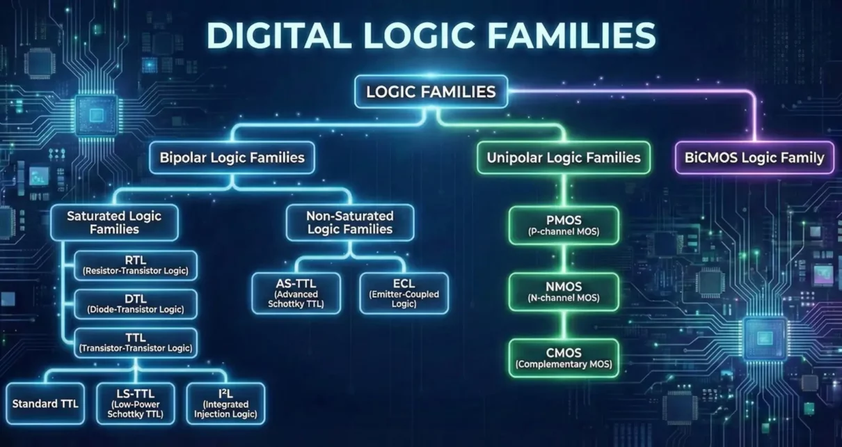
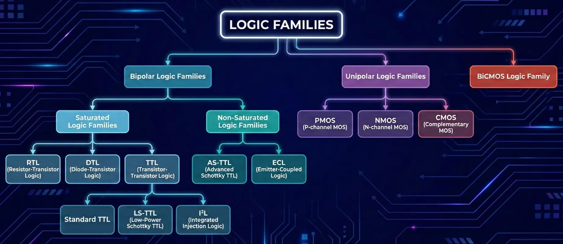
Classification of Logic Families
Logic families are broadly classified based on the type of active device used in their internal circuitry.
1. Bipolar (BJT-based) Logic Families
Use bipolar junction transistors. Generally fast but higher power consumption.
- RTL – Resistor-Transistor Logic
- DTL – Diode-Transistor Logic
- TTL – Transistor-Transistor Logic
- Standard TTL
- Schottky TTL (S-TTL)
- Low-power Schottky TTL (LS-TTL)
- Advanced Schottky TTL (AS-TTL)
- ECL – Emitter-Coupled Logic (very high speed)
- I²L – Integrated Injection Logic
2. MOS (Unipolar) Logic Families
Use MOSFETs. Lower power, higher packing density.
- PMOS
- Uses p-channel MOSFETs
- Slower, mostly obsolete
- NMOS
- Uses n-channel MOSFETs
- Faster than PMOS, moderate power
- CMOS – Complementary MOS
- Uses both PMOS and NMOS
- Very low power consumption
- High noise immunity
- Most widely used today
- 4000 series CMOS
- 74HC, 74HCT
3. BiCMOS Logic Family
- Combination of BJT + CMOS
- High speed (BJT) + low power (CMOS)
- Used in high-performance ICs
Comparison Table
| Family | Speed | Power | Popularity |
|---|---|---|---|
| RTL / DTL | Low | High | Obsolete |
| TTL | Medium | Medium | Older systems |
| ECL | Very High | Very High | Super high-speed |
| CMOS | Medium–High | Very Low | Most common |
| BiCMOS | High | Low | Specialized |
Key Characteristics of Logic Families
This section is the heart of digital logic family analysis. Each parameter directly affects real-world circuit performance.
Power Dissipation:
Power dissipation is the amount of power consumed by a logic gate during operation. It determines:
- Battery life in portable devices
- Heat generation
- Reliability of ICs
Bipolar logic families typically consume more power, even in static conditions, while CMOS consumes almost zero static power. Lower power dissipation is crucial for portable and high-density systems.
Propagation Delay:
Propagation delay is the time taken for a change at the input to reflect at the output of a logic gate.
- Measured in nanoseconds (ns)
- Determines the maximum operating frequency of a digital system
- Lower propagation delay means higher speed
ECL has the lowest propagation delay, while early MOS families are slower.
Fan-In:
Fan-in is the maximum number of inputs a logic gate can handle without performance degradation.
- Limited by input current and capacitance
- High fan-in increases complexity and delay
Fan-Out:
Fan-out is the number of logic gate inputs that a single output can drive reliably.
- Depends on output current capability
- Higher fan-out improves system expandability
TTL typically supports moderate fan-out, while CMOS supports very high fan-out.
Noise Margin:
Noise margin is the tolerance of a logic gate to unwanted voltage variations (noise).
- High noise margin = better noise immunity
- Crucial in industrial and high-speed environments
CMOS logic offers excellent noise margins compared to bipolar logic.
Operating Voltage:
Different logic families operate at different supply voltages:
- TTL: typically, 5 V
- CMOS: wide range (3 V to 15 V or more)
- ECL: negative supply voltages
Lower operating voltage leads to lower power consumption.
Power – Delay Product:
The power – delay product (PDP) represents the energy consumed per switching operation.
- PDP = Power Dissipation × Propagation Delay
- Lower PDP indicates a more efficient logic family
CMOS has the lowest PDP, making it ideal for modern systems.
Detailed Study of Major Logic Families
RTL and DTL Logic Family
1. Resistor – Transistor Logic (RTL)
Characteristics:
- Uses resistors to perform input logic operations
- Employs bipolar junction transistors (BJTs) for switching and amplification
- Basic logic gate implemented is NOR
- Transistor operates in cutoff and saturation regions
- Logic levels are represented by voltage variations
- Exhibits low noise margin
- Limited fan-out capability
- Simple circuit structure with low integration density
Advantages:
- Simple and easy to design
- Requires fewer components
- Low initial manufacturing cost
- Useful for understanding basic logic concepts
Disadvantages:
- Poor noise immunity
- High power dissipation due to continuous current flow
- Slow switching speed
- Not suitable for large-scale integration
Applications:
RTL was mainly used in early digital systems and is now limited to educational and historical significance, such as:
- Early generation computers
- Simple digital logic circuits
- Academic demonstrations
2. Diode – Transistor Logic (DTL)
Characteristics:
- Uses diodes to perform input logic operations
- Employs transistors for amplification and inversion
- Basic logic gate implemented is NAND
- Improved noise margin compared to RTL
- Better fan-in and fan-out capability
- Reduced interaction between input signals
- Moderate switching speed
- Higher reliability than RTL
Advantages:
- Better noise immunity than RTL
- Improved input isolation
- Higher operating speed compared to RTL
- More stable logic level operation
Disadvantages:
- Requires more components than RTL
- Higher power consumption than modern logic families
- Slower than TTL and CMOS due to transistor saturation
- Limited scalability for complex ICs
Applications:
DTL was used in:
- Early integrated circuits
- Industrial control systems
- Military and aerospace electronics (early generations)
Comparative Overview of RTL and DTL
| Parameter | RTL | DTL |
|---|---|---|
| Input logic elements | Resistors | Diodes |
| Basic gate | NOR | NAND |
| Noise immunity | Low | Moderate |
| Switching speed | Slow | Moderate |
| Power dissipation | High | Moderate |
| Circuit complexity | Very low | Moderate |
RTL and DTL logic families played a crucial role in the evolution of digital electronics. Although they have been replaced by advanced logic families such as TTL and CMOS, they remain important for understanding fundamental design trade-offs involving noise margin, power dissipation, and circuit complexity.
Transistor – Transistor Logic (TTL)
Transistor–Transistor Logic (TTL) is a bipolar logic family in which transistors are used for both logic operations and amplification. TTL employs a multi-emitter transistor at the input stage and typically uses the NAND gate as its fundamental building block. Due to its high speed, reliability, and well-defined logic levels, TTL became the most widely used logic family before the dominance of CMOS technology.
TTL circuits operate with a nominal 5 V power supply and offer better noise immunity, fan-out, and propagation delay compared to earlier logic families such as RTL and DTL.
General Characteristics of TTL
The common characteristics applicable to all TTL families are listed below:
- Logic Voltage Levels: Logic HIGH: 2 V to 5 V and Logic LOW: 0 V to 0.8 V
- Propagation Delay: TTL exhibits low propagation delay, making it suitable for high-speed digital circuits.
- Power Dissipation: Power dissipation varies with the TTL subfamily, with Standard TTL dissipating about 10 mW per gate.
- Noise Margin: TTL provides a noise margin of approximately 0.4 V, ensuring reasonable noise immunity.
- Fan-Out: A typical TTL gate has a fan-out of 10, which may be higher in advanced TTL variants.
- Supply Voltage: TTL requires a supply voltage in the range of 4.75 V to 5.25 V, with 5 V as the nominal value.
- Speed: TTL is known for its fast-switching speed compared to RTL and DTL.
- Compatibility: TTL devices are fully compatible with other TTL devices, allowing easy interconnection.
TTL Logic Families
1. Standard TTL
Characteristics:
- Uses BJTs for logic and amplification
- Multi-emitter input transistor
- NAND is the basic gate
- Typical propagation delay of about 10 ns
- Power dissipation of approximately 10 mW per gate
- Fan-out of 10
- Moderate switching speed
Advantages:
- Better speed and noise immunity than RTL and DTL
- Well-defined logic levels
- Widely standardized and documented
Disadvantages:
- Higher power consumption
- Slower than Schottky-based TTL
- Transistor saturation limits speed
Applications:
- Early digital computers
- Control logic circuits
- Medium-speed digital systems
2. Schottky TTL (S-TTL)
Characteristics:
- Uses Schottky diodes to prevent transistor saturation
- Very low propagation delay of about 3 ns
- High switching speed
- Power dissipation of approximately 20 mW per gate
- Fan-out of 10
- Operates at standard TTL voltage levels
Advantages:
- Very high speed
- Reduced storage delay
- Suitable for high-frequency applications
Disadvantages:
- High power consumption
- Increased heat dissipation
- Less suitable for low power design
Applications:
- High-speed digital circuits
- Data processing systems
- Fast control logic
3. Low-Power Schottky TTL (LS-TTL)
Characteristics:
- Combines Schottky clamping with power-reduction techniques
- Typical propagation delay of about 9 ns
- Low power dissipation of approximately 2 mW per gate
- Improved fan-out, typically 20
- Compatible with all TTL logic levels
- Widely used TTL subfamily
Advantages:
- Excellent balance between speed and power
- Reduced heat generation
- High reliability
Disadvantages:
- Slower than S-TTL and AS-TTL
- Higher power consumption than CMOS
Applications:
- General-purpose digital systems
- Microprocessor support logic
- Memory interfacing circuits
4. Advanced Schottky TTL (AS-TTL)
Characteristics:
- Uses optimized Schottky transistors
- Extremely low propagation delay of 1.5–2 ns
- Power dissipation of approximately 8 mW per gate
- High fan-out capability (≥ 20)
- Very high switching speed
Advantages:
- Excellent speed–power performance
- Suitable for high-performance systems
- Improved efficiency compared to earlier TTL families
Disadvantages:
- More complex circuit design
- Higher cost
- Still consumes more power than CMOS
Applications:
- High-speed arithmetic and logic units
- Advanced control systems
- High-performance digital electronics
Comparative Summary of TTL Families
| Parameter | Standard TTL | S-TTL | LS-TTL | AS-TTL |
|---|---|---|---|---|
| Propagation delay | ~10 ns | ~3 ns | ~9 ns | ~1.5–2 ns |
| Switching speed | Moderate | Very high | High | Very high |
| Power dissipation | ~10 mW | ~20 mW | ~2 mW | ~8 mW |
| Power consumption (relative) | High | Very high | Low | Moderate |
| Fan-out | 10 | 10 | 20 | ≥20 |
| Noise immunity | Good | Good | Good | Good |
| Transistor saturation | Yes | No | Reduced | No |
| Supply voltage | 5 V ±5% | 5 V ±5% | 5 V ±5% | 5 V ±5% |
| Common usage | Early systems | High-speed logic | General-purpose systems | High-performance systems |
The evolution of TTL from Standard TTL to Advanced Schottky TTL reflects continuous efforts to increase switching speed while reducing power dissipation, all while maintaining compatibility. Although CMOS has replaced TTL in most modern applications, TTL remains essential for understanding bipolar logic design and the historical development of digital systems.
ECL – Emitter-Coupled Logic Family
Emitter-Coupled Logic (ECL) is a high-speed bipolar logic family designed to overcome the switching speed limitations caused by transistor saturation in other logic families such as TTL. In ECL, transistors operate exclusively in the active region, which eliminates storage delay and results in extremely fast switching performance.
ECL circuits typically use differential amplifier configurations and a constant current source, making them suitable for very high-frequency and high-speed digital applications.
Characteristics of ECL:
- Logic Voltage Levels: Logic levels are defined by small voltage differences, typically around –0.8 V (logic HIGH) and –1.6 V (logic LOW).
- Propagation Delay: ECL exhibits extremely low propagation delay, typically in the range of 0.5 ns to 2 ns.
- Power Dissipation: ECL has high power dissipation due to continuous current flow, independent of switching activity.
- Noise Margin: ECL provides a moderate noise margin and requires careful layout due to small voltage swings.
- Fan-Out: ECL supports high fan-out capability because of its low output impedance emitter-follower outputs.
- Supply Voltage: ECL typically operates with a negative power supply of –5.2V.
- Speed: ECL is renowned for its extremely high switching speed among bipolar logic families.
- Transistor Operation: Transistors in ECL operate only in the active region and never enter saturation.
- Compatibility: ECL is not directly compatible with TTL or CMOS logic families without level-shifting circuits.
Advantages of ECL:
- Extremely high switching speed
- Minimal propagation delay
- No transistor saturation
- High fan-out capability
- Suitable for high-frequency and high-performance systems
Disadvantages of ECL:
- Very high-power consumption
- Requires a negative power supply
- Lower noise margin compared to CMOS
- Complex circuit design
- Higher cost and heat dissipation
Applications of ECL:
ECL is used in applications where speed is the primary requirement, such as:
- High-speed processors
- Supercomputers
- High-frequency communication systems
- Microwave and RF digital circuits
- High-speed instrumentation
Although ECL is rarely used in modern low-power digital systems due to its high-power consumption, it remains an important logic family for understanding high-speed bipolar circuit design. The principles of differential signaling and non-saturating transistor operation used in ECL have influenced modern high-speed logic and communication circuit designs.
Here’s the I²L section written to match your article exactly — same colon-style, single-line characteristics, same depth, and clean academic flow.
I²L – Integrated Injection Logic
Integrated Injection Logic (I²L), also known as IIL, is a low-power bipolar logic family that uses current injection instead of resistive loads to drive multiple logic gates. I²L was developed to achieve high integration density and very low power consumption, making it suitable for large-scale integrated circuits.
In I²L, transistors operate mainly in the saturation region, and logic functions are implemented using current steering techniques rather than voltage-level switching.
Characteristics of I²L:
- Logic Voltage Levels: Logic levels are defined by low-voltage operation, typically around 0.8 V (logic HIGH) and 0.2 V (logic LOW).
- Propagation Delay: I²L exhibits relatively high propagation delay compared to TTL and ECL due to saturated transistor operation.
- Power Dissipation: I²L has very low power dissipation, often in the microwatt range per gate.
- Noise Margin: I²L provides low noise margin due to small voltage swings.
- Fan-Out: I²L supports very high fan-out, as a single injector can drive many logic gates.
- Supply Voltage: I²L operates at a low supply voltage, typically between 0.8V and 1.5V.
- Speed: I²L has low switching speed compared to TTL and ECL.
- Integration Density: I²L offers very high packing density because it does not require resistors.
- Transistor Operation: Transistors in I²L operate primarily in the saturation region.
- Compatibility: I²L is not directly compatible with TTL or CMOS logic families.
Advantages of I²L:
- Very low power consumption
- High integration density
- Requires fewer components
- Simple circuit structure
- Suitable for large-scale integration
Disadvantages of I²L:
- Low switching speed
- Poor noise immunity
- High propagation delay
- Limited use in high-speed systems
Applications of I²L:
I²L is mainly used in applications where low power and high integration density are more important than speed, such as:
- Large-scale integrated circuits
- Low-power digital systems
- Portable electronic devices (early designs)
- Memory and control circuits
Although I²L is rarely used in modern digital designs, it played an important role in the development of low-power bipolar logic techniques. Many of its concepts influenced later low-power logic families and integration strategies.
MOS (Unipolar) Logic Families
MOS (Metal-Oxide-Semiconductor) logic families use MOSFETs as the primary switching devices instead of bipolar transistors. These logic families are known for low power consumption, high packing density, and large-scale integration capability. Because MOSFETs are voltage-controlled devices, MOS logic circuits draw significantly less power compared to bipolar logic families.
MOS logic families are broadly classified into PMOS, NMOS, and CMOS.
1. PMOS Logic Family:
PMOS logic uses p-channel MOSFETs as the switching elements. It was one of the earliest MOS logic families but has largely become obsolete due to its slow speed and higher power dissipation compared to NMOS and CMOS.
Characteristics of PMOS:
- Logic Device: Uses p-channel MOSFETs.
- Logic Voltage Levels: Logic levels are defined with respect to the supply voltage, with relatively large voltage swings.
- Propagation Delay: PMOS exhibits high propagation delay due to low hole mobility.
- Power Dissipation: Power dissipation is higher than CMOS and NMOS.
- Noise Margin: PMOS provides moderate noise margin.
- Fan-Out: PMOS supports moderate fan-out.
- Supply Voltage: PMOS typically operates at higher supply voltages.
- Speed: PMOS has low switching speed.
- Integration Density: Packing density is lower compared to NMOS and CMOS.
- Compatibility: PMOS is not compatible with modern MOS logic families.
Advantages of PMOS:
- Simple circuit design
- Early MOS implementation experience
Disadvantages of PMOS:
- Slow switching speed
- Higher power consumption
- Largely obsolete
Applications of PMOS:
- Early MOS integrated circuits
- Historical microprocessor designs
2. NMOS Logic Family:
NMOS logic employs n-channel MOSFETs, offering higher speed and better performance than PMOS due to higher electron mobility.
Characteristics of NMOS:
- Logic Device: Uses n-channel MOSFETs.
- Logic Voltage Levels: Logic levels are defined by the supply voltage and threshold voltage of NMOS devices.
- Propagation Delay: NMOS exhibits moderate propagation delay, faster than PMOS.
- Power Dissipation: NMOS has moderate static power dissipation.
- Noise Margin: NMOS provides moderate noise immunity.
- Fan-Out: NMOS supports higher fan-out than PMOS.
- Supply Voltage: NMOS typically operates with a single positive supply voltage.
- Speed: NMOS has higher switching speed than PMOS.
- Integration Density: Packing density is higher than PMOS.
- Compatibility: NMOS is not directly compatible with TTL without interfacing.
Advantages of NMOS:
- Faster operation than PMOS
- Higher packing density
- Simpler fabrication compared to CMOS
Disadvantages of NMOS:
- Higher power dissipation than CMOS
- Generates more heat
- Limited noise immunity compared to CMOS
Applications of NMOS:
- Early microprocessors
- Memory circuits
- Medium-speed digital systems
3. CMOS – Complementary MOS Logic Family:
CMOS logic uses both PMOS and NMOS transistors in a complementary arrangement, ensuring that power is consumed only during switching. Due to its very low power consumption, high noise immunity, and excellent scalability, CMOS is the most widely used logic family today.
Characteristics of CMOS:
- Logic Device: Uses complementary PMOS and NMOS transistors.
- Logic Voltage Levels: Logic levels span nearly the full supply voltage range.
- Propagation Delay: CMOS exhibits low propagation delay, improving with scaling.
- Power Dissipation: CMOS has extremely low static power dissipation.
- Noise Margin: CMOS provides very high noise immunity.
- Fan-Out: CMOS supports very high fan-out.
- Supply Voltage: CMOS operates over a wide range of supply voltages.
- Speed: CMOS offers high switching speed in modern devices.
- Integration Density: CMOS provides extremely high packing density.
- Compatibility: CMOS is compatible with other CMOS families and can be TTL-compatible in certain variants.
CMOS Subfamilies:
4000 Series CMOS:
- Technology: Standard CMOS technology.
- Supply Voltage: Operates over a wide range, typically 3 V to 15 V.
- Speed: Lower switching speed compared to HC series.
- Power Dissipation: Very low power consumption.
- Noise Immunity: Excellent noise margin.
- Applications: Low-speed, low-power digital systems.
74HC and 74HCT CMOS:
- 74HC (High-Speed CMOS):
- High switching speed comparable to TTL
- Very low power consumption
- CMOS input voltage levels
- 74HCT (High-Speed CMOS, TTL-Compatible):
- TTL-compatible input voltage levels
- Low power consumption
- Used for interfacing CMOS with TTL systems
Advantages of MOS Logic Families:
- Low power consumption
- High integration density
- Suitable for VLSI and ULSI designs
- Wide operating voltage range (CMOS)
Disadvantages of MOS Logic Families:
- Sensitive to electrostatic discharge (ESD)
- Slower than ECL in high-speed applications
- PMOS and NMOS are largely obsolete
Applications of MOS Logic Families:
- Microprocessors and microcontrollers
- Memory devices
- Digital signal processors
- Portable and battery-operated devices
- Modern digital and embedded systems
The transition from PMOS and NMOS to CMOS represents a major milestone in digital electronics. Today, CMOS dominates nearly all modern digital systems due to its unmatched combination of low power consumption, high noise immunity, and scalability.
BiCMOS Logic Family
BiCMOS (Bipolar CMOS) is a logic family that combines bipolar junction transistors (BJTs) and CMOS transistors on the same integrated circuit. This hybrid approach leverages the high switching speed and strong drive capability of BJTs together with the low power consumption and high integration density of CMOS.
BiCMOS technology is particularly suited for high-performance integrated circuits where both speed and power efficiency are critical design requirements.
Characteristics of BiCMOS:
- Logic Devices: Uses both BJTs and CMOS transistors in a single integrated circuit.
- Logic Voltage Levels: Logic levels are generally CMOS-compatible, allowing wide noise margins.
- Propagation Delay: BiCMOS exhibits lower propagation delay than pure CMOS due to bipolar drive capability.
- Power Dissipation: Power consumption is lower than TTL and ECL, but higher than pure CMOS.
- Noise Margin: BiCMOS provides high noise immunity, comparable to CMOS.
- Fan-Out: BiCMOS supports high fan-out because BJTs provide strong output drive currents.
- Supply Voltage: BiCMOS typically operates at CMOS supply voltages (commonly around 5 V or lower).
- Speed: BiCMOS offers high switching speed, approaching that of bipolar logic families.
- Integration Density: Integration density is higher than bipolar logic but slightly lower than pure CMOS.
- Compatibility: BiCMOS is compatible with CMOS logic levels and can interface with TTL using appropriate design.
Advantages of BiCMOS:
- Combines high speed of BJTs with low power of CMOS
- High output drive capability
- Improved performance in high-frequency applications
- Better noise immunity than bipolar logic families
Disadvantages of BiCMOS:
- More complex fabrication process
- Higher cost than pure CMOS
- Lower packing density than CMOS
- Design complexity is higher
Applications of BiCMOS:
BiCMOS is used in applications requiring both high speed and low power consumption, such as:
- High-performance microprocessors
- Analog–digital mixed-signal ICs
- High-speed I/O circuits
- RF and communication ICs
- Precision timing and control circuits
Although CMOS dominates most digital applications today, Bi-CMOS remains highly relevant in performance-critical and mixed-signal designs, where the superior drive strength of BJTs complements the power efficiency of CMOS.
Advantages of Logic Families
- Enable systematic implementation of digital logic circuits
- Provide different trade-offs between speed, power consumption, and noise immunity
- Allow designers to choose logic families based on application requirements
- Support a wide range of operating voltages and frequencies
- Facilitate integration from small-scale to very-large-scale systems
Disadvantages of Logic Families
- No single logic family optimally satisfies all performance parameters
- High-speed logic families often suffer from high power dissipation
- Low-power logic families may have limited switching speed
- Compatibility issues may arise between different logic families
- Certain logic families require complex fabrication and careful design
Applications of Logic Families
Logic families are used across almost all digital electronic systems, including:
- Microprocessors and microcontrollers
- Memory and storage devices
- Digital signal processors
- Communication and networking systems
- Control and automation systems
- Embedded and real-time systems
- Consumer electronics and portable devices
- High-performance computing systems
Conclusion
Logic families form the foundation of digital electronics by defining the electrical, performance, and functional characteristics of logic circuits. From early bipolar logic families such as RTL and TTL to modern CMOS and BiCMOS technologies, each logic family has contributed to the evolution of digital system design.
While bipolar logic families offer high speed, MOS logic families provide low power consumption and high integration density. Hybrid technologies such as BiCMOS bridge the gap by combining the advantages of both. The selection of an appropriate logic family ultimately depends on system requirements such as speed, power efficiency, noise immunity, cost, and scalability.
Short Questions and Answers on Logic Families
Q1. What is a logic family?
A logic family is a group of digital integrated circuits that share common electrical characteristics such as supply voltage, logic levels, power dissipation, and switching speed.
Q2. Why are logic families required in digital electronics?
Logic families ensure compatibility between logic gates and allow designers to select circuits based on speed, power consumption, noise immunity, and application requirements.
Q3. What is the basic logic gate of TTL?
The basic logic gate of TTL is the NAND gate.
Q4. Why is Schottky TTL faster than Standard TTL?
Schottky TTL prevents transistor saturation using Schottky diodes, thereby eliminating storage delay and increasing switching speed.
Q5. Why does ECL have the highest switching speed?
ECL transistors operate only in the active region and never enter saturation, resulting in extremely low propagation delay.
Q6. Why does ECL use a negative power supply?
A negative power supply reduces noise, improves speed, and helps maintain stable logic levels in high-speed operation.
Q7. What is Integrated Injection Logic (I²L)?
I²L is a low-power bipolar logic family that uses current injection instead of resistive loads, enabling high integration density.
Q8. Why does I²L have low power consumption but low speed?
I²L operates with saturated transistors and low voltage swings, which reduces power consumption but increases propagation delay.
Q9. Why are PMOS and NMOS logic families largely obsolete?
PMOS is slow and power-hungry, while NMOS consumes more power than CMOS. CMOS offers better speed, power efficiency, and noise immunity.
Q10. Why is CMOS the most widely used logic family today?
CMOS offers extremely low power consumption, high noise immunity, high packing density, and wide operating voltage range.
Q11. What is the difference between 74HC and 74HCT CMOS families?
74HC uses CMOS voltage levels, while 74HCT provides TTL-compatible input voltage levels.
Q12. What is BiCMOS technology?
BiCMOS combines bipolar junction transistors and CMOS transistors on the same chip to achieve high speed and low power consumption.
Q13. Why is BiCMOS preferred over pure CMOS in some applications?
BiCMOS provides higher drive capability and faster switching speed, making it suitable for high-performance and mixed-signal ICs.
Q14. What is fan-out and does it have a unit?
Fan-out is the maximum number of logic inputs driven by one logic output. It has no unit and is a dimensionless quantity.
Q15. Which logic family is preferred for high-speed applications?
ECL is preferred for extremely high-speed applications, while BiCMOS is used where both high speed and low power are required.
Types of Diodes with Symbol, Definition, Working and Applications
Types of Transistors: Classification (BJT, JFET, MOSFET & IGBT)
Types of Resistors with Symbol, Classification and Applications
