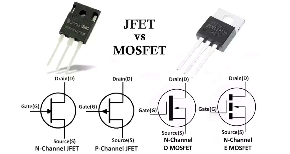
Field Effect Transistors (FETs) are vital components in modern electronics, widely used in amplification, switching, and signal modulation. The two primary types of FETs are the Junction Field Effect Transistor (JFET) and the Metal-Oxide-Semiconductor Field Effect Transistor (MOSFET). This article explains the difference between JFET and MOSFET based on their types, construction, characteristics, advantages, disadvantages and applications with a detailed comparison table to provide a comprehensive understanding of their roles in electronics.
What is a JFET?
A Junction Field Effect Transistor (JFET) is a voltage-controlled semiconductor device where the flow of current between the source and drain is regulated by the voltage applied to the gate. Unlike bipolar junction transistors (BJTs), which are current-controlled devices, JFETs are controlled entirely by electric fields.
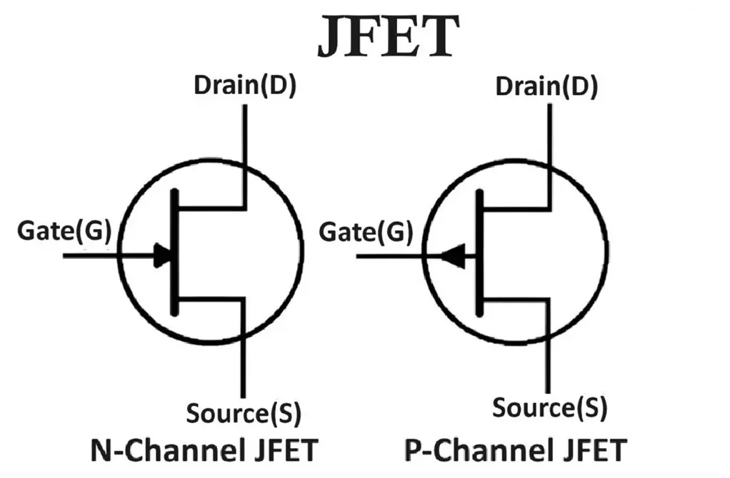
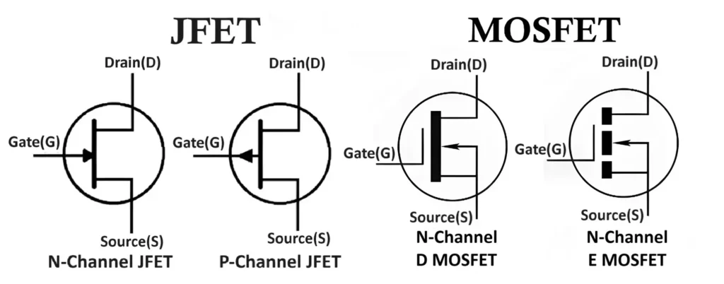
Types of JFET
N-Channel JFET:
- Uses N-type material for the channel.
- Electrons are the majority carriers, providing higher conductivity compared to P-channel JFETs.
P-Channel JFET:
- Uses P-type material for the channel.
- Holes are the majority carriers, resulting in slightly lower conductivity than N-channel JFETs.
Construction of JFET
- Source (S): The terminal through which current enters the channel. It serves as the starting point for electron or hole flow.
- Drain (D): The terminal where current exits the channel. The drain voltage relative to the source determines the current flow magnitude.
- Gate (G): A control terminal that modulates the width of the channel by applying voltage. The gate is reverse-biased with respect to the channel, creating a depletion region.
- Channel: A semiconductor pathway (N-type or P-type) that allows current to flow between the source and drain. The conductivity of the channel is controlled by the gate voltage.
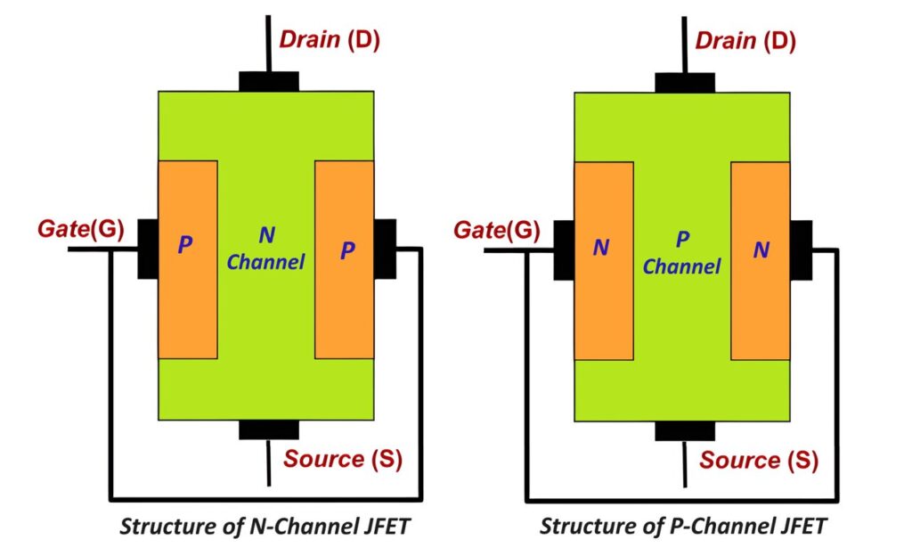
In JFETs, the gate forms a PN junction with the channel. The reverse biasing of this junction narrows the channel and restricts the current flow, enabling voltage-controlled operation.
Characteristics of JFET
High Input Impedance:
The reverse-biased PN junction at the gate offers high resistance, resulting in minimal input current.
Current Saturation:
After a certain point, increasing the drain-source voltage (VDS) does not increase the drain current (ID).
Depletion Mode Operation:
The JFET operates only in depletion mode, where the application of gate voltage reduces current flow.
Advantages of JFET
- Low power consumption.
- High input impedance.
- Simple construction and design.
- Low noise performance, making it suitable for audio applications.
Disadvantages of JFET
- Limited control over current flow compared to MOSFETs.
- Lower gain and slower switching speed.
- Operates only in depletion mode.
Applications of JFET
- Low-noise amplifiers, such as in audio systems and instrumentation.
- Impedance matching circuits.
- Analog signal processing.
- Oscillator circuits in RF applications.
Example JFETs:
- 2N3819 (N-Channel JFET)
- J310 (N-Channel JFET)
What is a MOSFET?
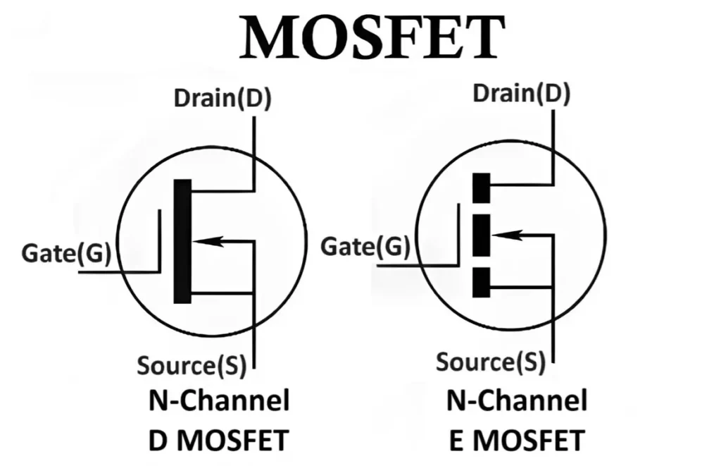
A Metal-Oxide-Semiconductor Field Effect Transistor (MOSFET) is a voltage-controlled device with an insulated gate that controls the conductivity of a semiconductor channel. MOSFETs are more versatile and widely used in both analog and digital applications.
Types of MOSFET
Enhancement Mode MOSFET (E MOSFET):
- The device is off at zero gate voltage. The channel is formed only when a threshold voltage is applied to the gate.
Depletion Mode MOSFET (D MOSFET):
- The device is on at zero gate voltage, and applying a voltage to the gate narrows or depletes the channel.
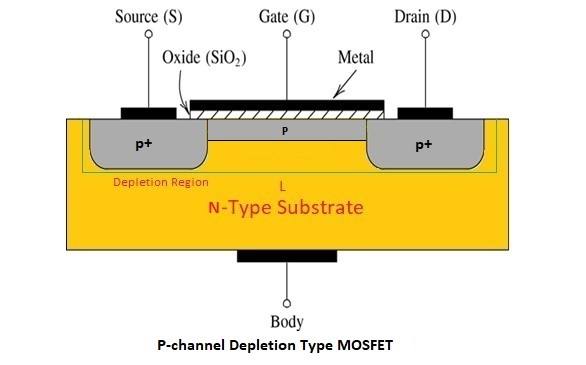
Construction of MOSFET
- Source (S): The terminal where current enters the channel. In MOSFETs, current flows due to the movement of majority charge carriers (electrons in N-channel or holes in P-channel).
- Drain (D): The terminal where current exits the channel. The voltage applied at the drain relative to the source determines the current flow magnitude.
- Gate (G): The control terminal insulated from the channel by a thin layer of silicon dioxide (SiO2). This insulation allows for extremely high input impedance.
- Channel: The conductive path between the source and drain, formed or depleted based on the gate voltage. Channels can be of N-type or P-type material.
- Body (B): The substrate on which the MOSFET is fabricated. It is typically connected to the source terminal to prevent unwanted voltage variations.
- Insulating Layer: A thin dielectric layer (typically SiO2) that insulates the gate from the channel, enabling voltage control with minimal gate current.
The insulated gate allows for extremely high input impedance, making MOSFETs ideal for high-frequency and digital applications.
Characteristics of MOSFET
High Input Impedance:
The insulating layer ensures negligible gate current, resulting in extremely high impedance.
Dual-Mode Operation:
Operates in both enhancement and depletion modes, offering greater flexibility.
Faster Switching Speeds:
The low gate capacitance and high mobility of charge carriers enable rapid switching.
Advantages of MOSFET
- High switching speed.
- Low power consumption during steady-state operation.
- High input impedance, making it suitable for sensitive circuits.
- Versatility in digital and analog applications.
Disadvantages of MOSFET
- Susceptible to damage from electrostatic discharge (ESD).
- Higher noise levels compared to JFETs.
- More complex structure and costlier to manufacture.
Applications of MOSFET
- Power electronics, such as inverters and converters.
- Switching devices in digital circuits (e.g., CMOS technology).
- RF amplifiers.
- Motor control and LED drivers.
- Battery management systems in electric vehicles.
- High-efficiency power supplies.
Example MOSFETs:
- IRF540N (N-Channel Power MOSFET)
- BS170 (Small-Signal N-Channel MOSFET)
- IRF9540 (P-Channel Power MOSFET)
Difference Between JFET and MOSFET
| Aspect | JFET | MOSFET |
|---|---|---|
| Structure | Simpler structure with a single semiconductor material and a PN junction between Gate and channel. | Includes an insulating SiO2 layer between Gate and channel, with four terminals: Gate, Source, Drain, and Body. |
| Operating Modes | Operates only in depletion mode; Gate voltage narrows the channel to reduce current flow. | Operates in both enhancement and depletion modes; Gate voltage can either enhance or deplete channel conductivity. |
| Input Impedance | High, due to the reverse-biased PN junction, but lower compared to MOSFET. | Extremely high, thanks to the insulating SiO2 layer, ideal for high-impedance applications. |
| Power Consumption | Low power consumption during operation due to minimal current at the Gate. | Low during steady-state operation, but switching at high frequencies can cause increased power loss. |
| Switching Speed | Relatively slow, making it more suitable for analog applications like amplifiers. | Very fast, suitable for high-speed and high-frequency applications such as power electronics and microprocessors. |
| Noise Performance | Low noise, ideal for applications like audio preamplifiers and instrumentation amplifiers. | Higher noise levels, though advancements in design have mitigated this in modern MOSFETs. |
| Robustness | More robust and less sensitive to electrostatic discharge (ESD) and voltage spikes. | More sensitive to ESD and over-voltage, requiring protective handling and circuits. |
| Examples | 2N3819, J310 | IRF540N, BS170, IRF9540 |
| Applications | Low-noise amplifiers, impedance buffers, RF oscillators, and analog signal processing. | Power electronics, switching circuits, digital logic circuits, battery management systems, motor drivers, and LED control systems. |
| Cost and Availability | Generally cheaper and simpler to manufacture, but less versatile in modern applications. | More expensive due to advanced construction but widely used in various electronic systems, especially high-power and high-frequency applications. |
Conclusion
JFETs and MOSFETs are indispensable in modern electronics, each excelling in different areas. JFETs are ideal for low-noise analog circuits and robust applications, whereas MOSFETs dominate high-speed digital and power electronics. Understanding the difference between JFET and MOSFET with their types, structures, characteristics, applications, and limitations ensures informed decisions when designing efficient and reliable electronic systems.
Types of Transistors: Classification (BJT, JFET, MOSFET & IGBT)
