A Buffer Gate is one of the fundamental building blocks in digital electronics. Unlike a NOT gate, it does not invert the signal, it simply passes the input to the output without changing its logic state.
In simple terms, a buffer gate produces an output that is identical to its input. If the input is HIGH (1), the output remains HIGH (1), and if the input is LOW (0), the output remains LOW (0).
Although it may seem trivial, the buffer plays a very important role in practical digital systems. It is mainly used for:
- Signal strengthening (driving capability)
- Isolation between circuit stages
- Improving signal integrity
- Increasing fan-out capacity
Buffers are widely used in microprocessors, memory systems, communication buses, and interfacing circuits, where a signal needs to be transmitted over longer distances or drive multiple loads.
They are essential because in real-world circuits, signals can degrade due to loading effects. A buffer ensures that the signal remains stable and strong without altering its logic state.
- Related Articles:
- Types of Logic Gates with Symbol, Truth Table and IC Numbers
- Universal NOR Gate Truth Table with IC 7402 PIN Diagram
- NAND Gate Truth Table, Logic Circuit & IC 7400 Pin Diagram
- OR Gate: Symbol, Truth Table, Logic Circuit, and IC Numbers
- AND Gate: Symbol, Truth Table, Logic Circuit, and IC Numbers
- NOT Gate: Symbol, Truth Table, Logic Circuit, and IC Numbers
- XOR Gate: Symbol, Truth Table, Logic Circuit, and IC Numbers
- XNOR Gate: Symbol, Truth Table, Logic Circuit, and IC Numbers
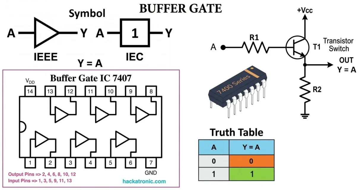
Symbol of Buffer Gate
- Standard Symbol (ANSI)
- The most commonly used symbol (ANSI standard) consists of:
- A triangle shape pointing towards the right
- No inversion bubble at the output (this is the key difference from NOT gate)
- One input line entering from the left
- One output line exiting from the right
- IEC Symbol
- Represented as a rectangle
- Inside marking: 1 (indicating unity gain / no inversion)
- Input enters from the left, output exits from the right
- No inversion bubble
- Single-Input Nature
- A buffer gate has only one input
- It does not perform logical operations like AND/OR
- The logic is fixed: output always follows input
- Terminal and Notation
- Input: A
- Output: Y or Q
- Boolean Expression: Y = A
- This indicates that the output is exactly equal to the input.
- Important Observations
- Absence of an inversion bubble distinguishes it from a NOT gate
- Output is always identical to the input
- Used primarily for signal amplification and isolation, not logic transformation
- Can be extended into tri-state buffers for bus control applications
- Helps in increasing fan-out without affecting the original signal source
Buffer Gate Truth Table
- Working Principle
- The buffer gate operates on a very simple condition:
- Output is HIGH (1) when the input is HIGH (1)
- Output is LOW (0) when the input is LOW (0)
- Unlike a NOT gate, which inverts the signal, a buffer preserves the logic state and provides a strengthened or isolated version of the input signal.
- Buffers do not evaluate multiple inputs like AND/OR gates, they simply replicate the input at the output with improved driving capability.
- The buffer gate operates on a very simple condition:
- Boolean Logic
- The buffer follows the fundamental Boolean identity: Y = A
- The output is exactly equal to the input
- No inversion or logical transformation occurs
- Because of this behavior, it is often referred to as a non-inverting gate.
- Key Condition
- Input = HIGH → Output = HIGH
- Input = LOW → Output = LOW
- If A = 1 → Y = 1
- If A = 0 → Y = 0
- Key Observation:
- The output is always identical to the input
- No inversion occurs (unlike NOT gate)
- No multi-input (same as NOT gate, single input only)
- Logic remains fixed: Output = Input
- It acts as a signal follower, not a logical operator
- The buffer is extremely useful in:
- Signal amplification (logic level restoration)
- Driving multiple loads
- Isolating sensitive circuit stages
Types of Buffer Gates
Standard Buffer (Non-Inverting Buffer)
- A standard buffer is the most basic type of buffer gate where the output directly follows the input without any control signal.
- Function: Y = A
- Key Features:
- Always active (no enable/disable control)
- Provides signal amplification (drive strength)
- Improves fan-out capability
- Helps in isolating stages of a circuit
- Typical Use:
- Between logic gates to prevent loading effects
- In long interconnections to maintain signal integrity
Tri-State Buffer
- A tri-state buffer introduces a third output state called High Impedance (Z) in addition to logic HIGH and LOW.
- Working:
- Enable = 1 → Output follows input
- Enable = 0 → Output = High Impedance (Z)
- Key Features:
- Can effectively disconnect itself from the circuit
- Enables multiple devices to share a common bus
- Prevents bus contention (signal conflicts)
- Types:
- Active HIGH enable
- Active LOW enable
- Typical Use:
- Data buses in microprocessors
- Memory interfacing systems
Inverting Buffer (Buffer Inverter)
- An inverting buffer combines the function of a buffer and a NOT gate.
- Function: Y = A’
- Key Features:
- Provides signal inversion + amplification
- Improves signal strength while changing logic state
- Faster switching compared to basic NOT gates in some IC families
- Typical Use:
- Signal conditioning where inversion is required
- Clock signal shaping
Open-Collector Buffer
- An open-collector buffer uses a transistor whose collector terminal is left open (not internally connected to Vcc).
- Working Principle:
- Output LOW → Transistor ON (pulls line to ground)
- Output HIGH → Transistor OFF (line pulled HIGH via external resistor)
- Key Features:
- Requires external pull-up resistor
- Allows multiple outputs to be connected together
- Supports wired-AND logic
- Advantages:
- Safe for interfacing different voltage levels
- Can drive higher voltage/current loads
- Typical Use:
- I²C communication lines
- Interrupt lines and shared signals
Open-Drain Buffer (CMOS Version)
- The open-drain buffer is the CMOS equivalent of the open-collector configuration.
- Key Features:
- Uses MOSFET instead of BJT
- Requires external pull-up resistor
- Lower power consumption
- Better suited for modern digital ICs
- Typical Use:
- Widely used in embedded systems
- Communication protocols like I²C
Bidirectional Buffer
- A bidirectional buffer allows signals to pass in both directions depending on a control signal.
- Working:
- Direction control determines input/output flow
- Often combined with tri-state control
- Key Features:
- Supports two-way data communication
- Includes direction (DIR) and enable (EN) pins
- Prevents data collision
- Typical Use:
- Data buses in microprocessors and memory systems
- GPIO expansion and interfacing
Schmitt Trigger Buffer
- A Schmitt trigger buffer introduces hysteresis, meaning it has two distinct threshold voltages:
- Upper threshold (VT+)
- Lower threshold (VT−)
- Key Features:
- Excellent noise immunity
- Converts slow or noisy signals into clean digital outputs
- Eliminates false triggering
- Advantages:
- Ideal for signals with gradual transitions
- Improves reliability in noisy environments
- Typical Use:
- Switch debouncing
- Signal conditioning
- Oscillator circuits
Bus Buffer / Line Driver
- A bus buffer (or line driver) is designed to drive large capacitive loads and long transmission lines.
- Key Features:
- High current sourcing and sinking capability
- Reduces signal degradation over distance
- Maintains signal timing and integrity
- Advantages:
- Supports high fan-out
- Improves propagation reliability
- Typical Use:
- Address/data buses
- Communication interfaces
- Backplane systems
Level Shifting Buffer
- A level shifting buffer is used to translate signals between different voltage domains.
- Key Features:
- Converts logic levels safely (e.g., 1.8V ↔ 3.3V ↔ 5V)
- Protects low-voltage devices from damage
- Can be uni-directional or bidirectional
- Challenges Solved:
- Voltage compatibility between devices
- Mixed-signal system integration
- Typical Use:
- Microcontroller to sensor interfacing
- Modern low-power digital systems
Clock Buffer
- A clock buffer is a specialized buffer designed specifically for distributing clock signals.
- Key Features:
- Minimizes clock skew
- Maintains signal timing accuracy
- Provides multiple synchronized outputs
- Advanced Variants:
- Zero-delay buffers
- PLL-based clock buffers
- Typical Use:
- CPUs and microcontrollers
- Synchronous digital systems
- FPGA and high-speed designs
Types of Buffer Gate
| Type | Core Function | Key Advantage | Common Application |
|---|---|---|---|
| Standard Buffer | Output = Input | Signal strengthening | General logic circuits |
| Tri-State Buffer | Adds High-Z state | Bus sharing | Data buses |
| Inverting Buffer | Output = NOT Input | Inversion + drive | Signal processing |
| Open-Collector | External pull-up | Wired logic capability | I²C, shared lines |
| Open-Drain | CMOS open-collector | Low power | Embedded systems |
| Bidirectional | Two-way data flow | Flexible communication | Data buses |
| Schmitt Trigger | Hysteresis | Noise immunity | Signal conditioning |
| Bus Buffer | High drive capability | Long-distance transmission | Memory, communication buses |
| Level Shifter | Voltage conversion | Device protection | Mixed-voltage systems |
| Clock Buffer | Clock distribution | Low skew | Processors, digital timing |
Buffer Gate Circuit Implementation
The buffer gate can be implemented using different hardware technologies. Although its logical function is simple (output = input), its practical implementations focus on improving drive strength, isolation, and signal integrity.
Each implementation differs in terms of speed, power consumption, voltage levels, and fan-out capability.
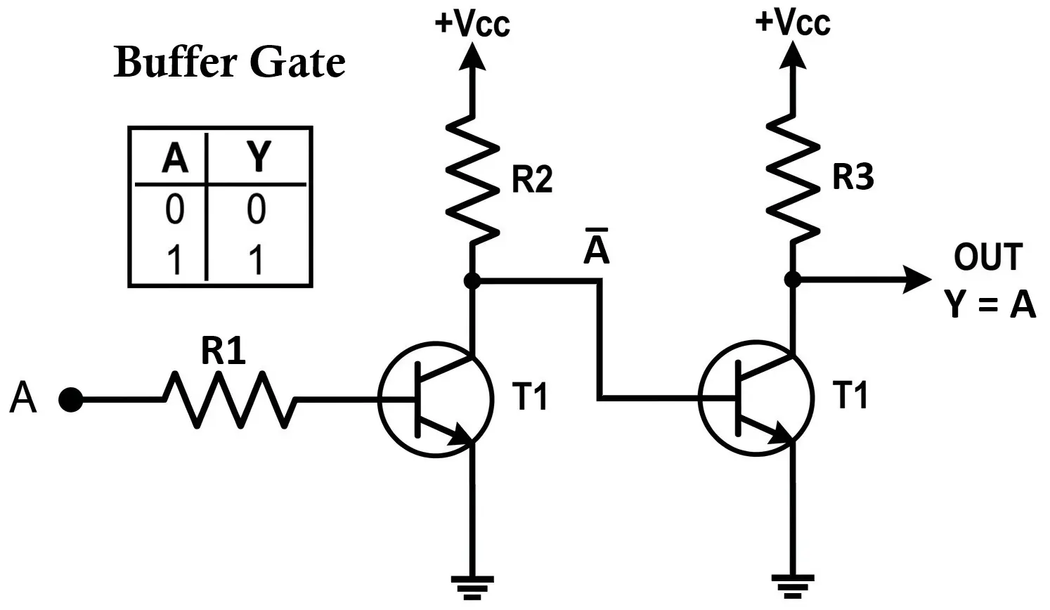
Transistor Buffer (Emitter Follower)
- A transistor used as a buffer operates in the active (linear) region.
- It behaves as an emitter follower (common collector):
- Output voltage ≈ Input voltage − VBE (0.7 V)
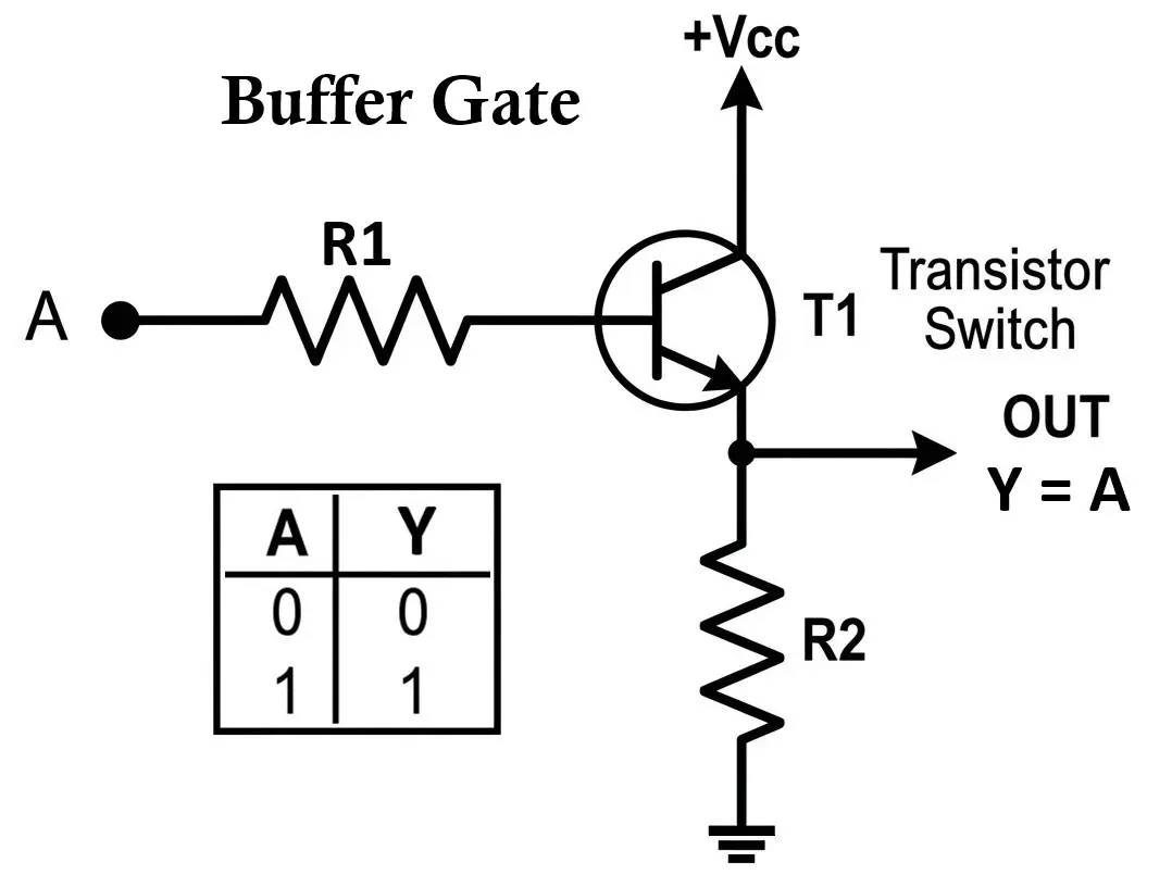
- Operation
- Input HIGH
- Transistor ON
- Emitter follows input
- Vout ≈ Vin − 0.7 V
- Input LOW
- Transistor OFF
- Output LOW
- Input HIGH
- Key Insight
- No inversion, and high input impedance, low output impedance
- Used for buffering and impedance matching
Two-Transistor Buffer (Collector Output Type)
- Both transistors operate mainly in common emitter configuration
- First transistor provides amplification
- Second transistor provides further gain and inversion
- Output is taken from collector → gives voltage gain and inversion
- Structure
- Input → base of Q1
- Q1 drives Q2
- Output is taken from collectors (typically Q2 collector)
- Operation
- Input HIGH
- Q1 ON → collector voltage LOW
- Q2 OFF → collector pulled HIGH
- Output = HIGH
- Input LOW
- Q1 OFF → collector pulled HIGH
- Q2 ON → collector pulled LOW
- Output = LOW
- Input HIGH
- Key Insight
- Output is taken from collector → always an inverting stage
- Each common-emitter stage gives inversion
- Two stages can result in:
- Single inversion (depending on coupling)
- Double inversion (non-inverting overall)
CMOS Buffer Gate (Double Inverter Circuit)
- Structure
- Two CMOS inverters connected in series:
- First inverter → inverts signal
- Second inverter → re-inverts signal
- Two CMOS inverters connected in series:
- Configuration
- Each inverter consists of:
- PMOS (pull-up)
- NMOS (pull-down)
- Each inverter consists of:
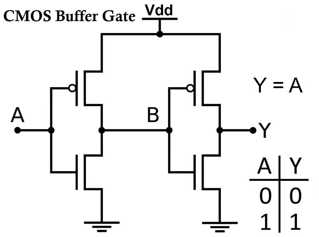
- Working
- Input LOW → first inverter outputs HIGH → second inverter outputs LOW → final output = input
- Input HIGH → first inverter outputs LOW → second inverter outputs HIGH → final output = input
- Advantages
- Very low power consumption
- High noise immunity
- Strong output drive capability
- Most widely used in modern digital ICs and VLSI systems
NAND-Based Buffer Gate
- Boolean Expression: Y = A
- Stepwise implementation:
- First NAND: Y1 = A’
- Second NAND: Y = Y1′ = (A’)’ = A
- Stepwise implementation:
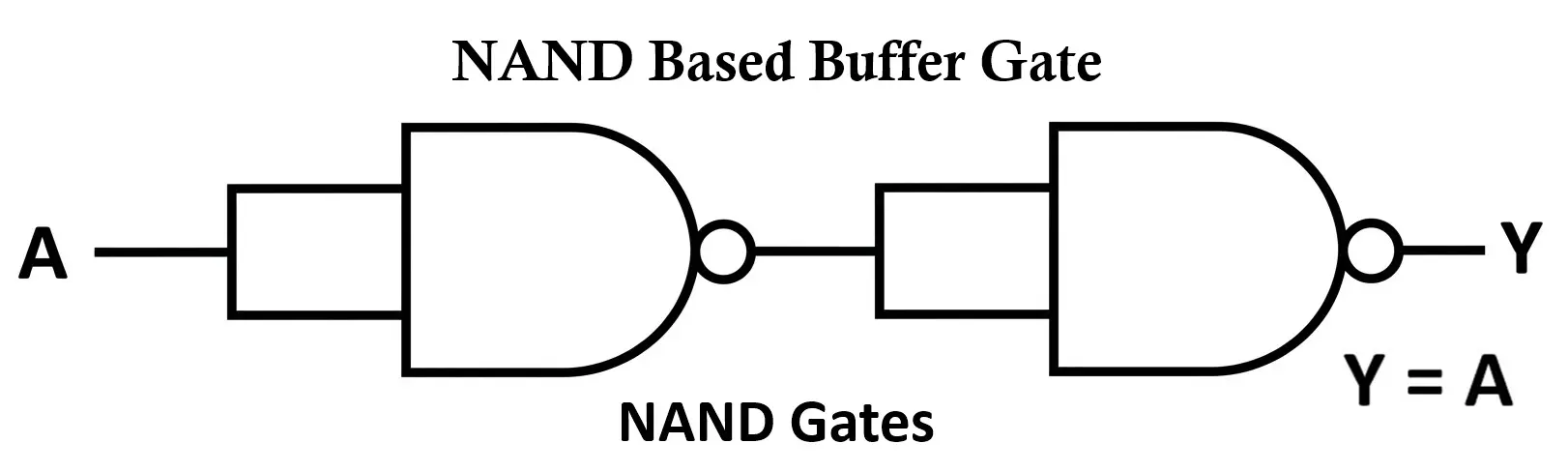
- Implementation
- Use two NAND gates
- First NAND acts as NOT
- Second NAND re-inverts to get original signal
- Key Insight
- NAND is a universal gate
- Buffer can be built using only NAND gates
- Useful in NAND-only digital designs
NOR-Based Buffer Gate
- Boolean Expression: Y = A
- Stepwise implementation:
- First NOR: Y1 = A’
- Second NOR: Y = Y1′ = (A’)’ = A
- Stepwise implementation:
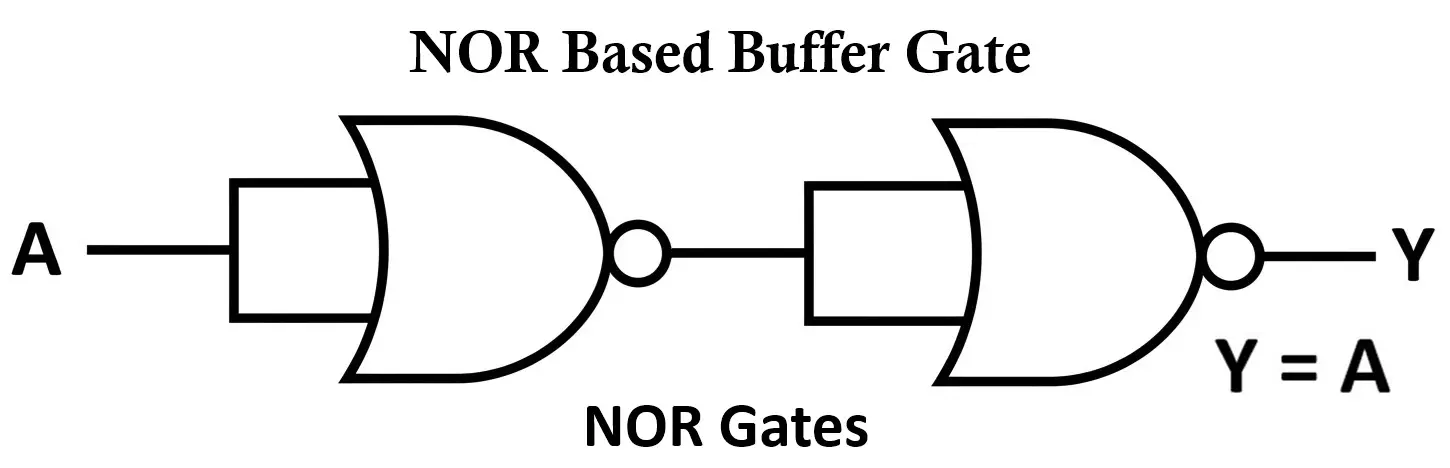
- Implementation
- Use two NOR gates
- First NOR inverts
- Second NOR restores original signal
- Key Insight
- NOR is also a universal gate
- Enables buffer design using only NOR gates
Tri-State Buffer
- Includes an Enable (EN) control input
- Operation
- EN = 1 → Output follows input (normal buffer operation)
- EN = 0 → Output becomes High Impedance (Z)
- Key Insight
- Allows multiple devices to share a common data bus
- Prevents signal conflict
- Widely used in:
- Microprocessors
- Memory interfacing
- Communication systems
IC Numbers and Details
Buffer gates are available in a wide range of ICs across TTL and CMOS families. These ICs are specifically designed to provide high drive capability, signal isolation, level shifting, and stable logic transmission without altering the logic level.
They are essential in real-world systems where fan-out, noise immunity, bus control, and voltage compatibility are critical.
7407 – Hex Buffer (Open Collector)
The 7407 IC is a widely used hex non-inverting buffer with open-collector outputs.
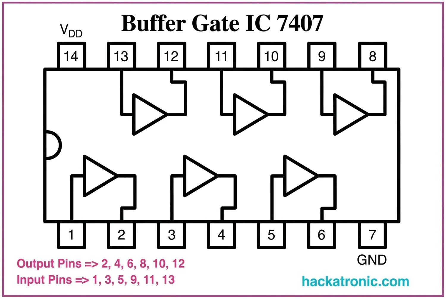
- Features
- 6 independent buffers
- Technology: TTL (BJT-based)
- Output type: Open collector
- Supply voltage: 5V
- Propagation delay: ~10–15 ns
- High current driving capability
- Pin Configuration
- Total pins: 14
- Buffers:
- 1A–1Y → Pins 1–2
- 2A–2Y → Pins 3–4
- 3A–3Y → Pins 5–6
- 4A–4Y → Pins 9–8
- 5A–5Y → Pins 11–10
- 6A–6Y → Pins 13–12
- Power:
- Pin 14: Vcc
- Pin 7: GND
- Key Characteristics
- Requires external pull-up resistor
- Can drive relays, LEDs, and higher loads
- Supports voltage level interfacing
7417 – Hex Buffer (High Voltage Open Collector)
The 7417 IC is similar to 7407 but designed for higher voltage operation.
- Specifications
- Technology: TTL
- Output: Open collector
- Propagation delay: ~10 ns
- Higher voltage handling capability
- Key Characteristics
- Suitable for industrial applications
- Can interface with higher voltage systems
74LS07 – Low-Power Schottky Buffer
The 74LS07 IC is an improved TTL buffer with lower power consumption and higher speed.
- Specifications
- Technology: Low-Power Schottky TTL
- Supply voltage: 5V
- Propagation delay: ~8–12 ns
- Output: Open collector
- Key Characteristics
- Better speed–power tradeoff
- Used in efficient TTL systems
74HC125 – Quad Tri-State Buffer (Active LOW Enable)
The 74HC125 IC is one of the most widely used tri-state buffer ICs in modern systems.
- Features
- 4 independent buffers
- CMOS technology
- Tri-state outputs (HIGH, LOW, High-Z)
- Very low power consumption
- High-speed operation
- Pin Configuration
- Total pins: 14
- Each buffer includes:
- Input (A)
- Output (Y)
- Enable (OE – active LOW)
- Power:
- Pin 14: Vcc
- Pin 7: GND
- Working
- OE = 0 → Output follows input (Y = A)
- OE = 1 → Output = High Impedance (Z)
- Key Characteristics
- Enables bus sharing
- Prevents bus contention
- Widely used in microprocessors and memory systems
74HC126 – Quad Tri-State Buffer (Active HIGH Enable)
The 74HC126 IC is similar to 74HC125 but uses active HIGH enable logic.
- Working
- OE = 1 → Output follows input
- OE = 0 → Output = High Impedance
- Key Difference
- 74HC125 → Active LOW
- 74HC126 → Active HIGH
74HC244 – Octal Buffer (Bus Buffer)
The 74HC244 IC is an 8-bit non-inverting buffer with tri-state outputs.
- Specifications
- Technology: CMOS
- Supply voltage: 2V to 6V
- Propagation delay: ~8–15 ns
- Dual enable pins
- Tri-state outputs
- Key Characteristics
- Used for address/data bus buffering
- Improves fan-out and signal integrity
- Provides isolation between system blocks
74HCT244 – TTL-Compatible CMOS Buffer
The 74HCT244 IC is a variant of HC244 with TTL-compatible input levels.
- Specifications
- CMOS technology with TTL compatibility
- Supply voltage: 5V
- Low power consumption
- Key Characteristics
- Bridges TTL and CMOS systems
- Eliminates need for external level shifting
74HC245 – Bidirectional Bus Transceiver
The 74HC245 IC is a bidirectional buffer (transceiver) used for controlled data transfer.
- Features
- 8-bit bidirectional buffer
- Direction control (DIR)
- Output enable (OE)
- Tri-state outputs
- Working
- DIR controls data direction (A ↔ B)
- OE enables/disables output
- Key Characteristics
- Used in microprocessors and memory systems
- Enables controlled two-way communication
CD4050 – CMOS Buffer (Level Shifter)
The CD4050 IC belongs to the 4000-series CMOS family and is widely used for level shifting.
- Specifications
- Supply voltage: 3V to 15V
- Extremely low power consumption
- High input impedance
- Key Characteristics
- Converts high voltage inputs to lower logic levels
- Ideal for battery-powered systems
- Protects sensitive devices
Buffer Gate ICs Comparison Table
| IC Number | Technology | Voltage Range | Speed | Output Type | Special Feature |
|---|---|---|---|---|---|
| 7407 | TTL | 5V | Medium | Open collector | High current drive |
| 7417 | TTL | 5V | Medium | Open collector | High voltage capability |
| 74LS07 | TTL (LS) | 5V | High | Open collector | Low power TTL |
| 74HC125 | CMOS | 2–6V | High | Tri-state | Active LOW enable |
| 74HC126 | CMOS | 2–6V | High | Tri-state | Active HIGH enable |
| 74HC244 | CMOS | 2–6V | High | Tri-state | Bus buffer |
| 74HCT244 | CMOS+TTL | 5V | High | Tri-state | TTL compatibility |
| 74HC245 | CMOS | 2–6V | High | Tri-state | Bidirectional |
| CD4050 | CMOS | 3–15V | Medium | Non-inverting | Level shifting |
Timing and Practical Considerations
- Propagation Delay
- Propagation delay is the time taken for the output to follow a change in input.
- TTL Buffers (e.g., 7407 IC): ~10–15 ns
- CMOS Buffers (e.g., 74HC125 IC): ~8–15 ns (can be lower in modern ICs)
- Although a buffer does not change logic, it introduces a small delay
- Critical in: High-frequency circuits, clock distribution networks and digital timing systems
- Fan-In and Fan-Out
- Fan-In
- Buffer gate has only one input
- Fan-in is fixed (same as NOT gate)
- Fan-Out
- Number of inputs a buffer output can drive
- TTL Buffers: ~10 loads
- CMOS Buffers: Much higher (due to high input impedance)
- Buffers are specifically used to increase fan-out
- Essential in systems where one signal drives multiple devices
- Fan-In
- Noise Margin
- CMOS Buffers > TTL Buffers
- CMOS provides better noise immunity
- Importance
- Reliable operation in:
- Industrial environments
- Embedded systems
- Long signal paths
- Reliable operation in:
- Power Consumption
- TTL Buffers: Higher power consumption
- CMOS Buffers: Extremely low (µW range)
- Preferred Usage
- CMOS buffers (like 74HC244 IC) are preferred for:
- Battery-powered devices
- Portable electronics
- Low-power embedded systems
Buffer Gate Example
- Signal Strengthening / Isolation
- Consider a system with one signal:
- Input signal (A)
- Output (Y) drives multiple loads
- The buffer ensures:
- Output remains identical to input
- Signal is strong enough to drive multiple circuits
- Consider a system with one signal:
| A | Y = A |
|---|---|
| 0 | 0 |
| 1 | 1 |
-
- Without buffer → signal may degrade
- With buffer → clean, strong, stable signal
Buffer Gate Circuit Implementations
- Using Switches (Mechanical Logic)
- Signal passed through switch-controlled path
- No inversion, only control of signal flow
- Used in:
- Basic control circuits
- Manual signal routing
- Using Relay Logic
- Relay configured to pass signal without inversion
- Acts as an electrical isolator
- Used in:
- Industrial control panels
- Power isolation systems
- Using FPGA / Digital Systems
- Implemented in HDL: assign Y = A;
- Often combined with enable signals (tri-state buffers)
- Used in: FPGA design, ASIC systems, high-speed digital logic
Applications of Buffer Gate
- Logic and Signal Processing
- Signal buffering
- Fan-out expansion
- Signal isolation
- Noise reduction
- Digital Electronics
- Bus interfacing (using 74HC125 IC, 74HC244 IC)
- Memory systems
- Register and counter circuits
- Data transmission lines
- Computing Systems
- CPU data buses
- Address buffering
- Memory interfacing
- I/O expansion
- Everyday Electronics
- LED driving circuits
- Signal conditioning
- Level shifting (using CD4050 IC)
- Communication interfaces
Advantages of Buffer Gate
- Simple and easy to implement
- Does not alter logic (non-inverting: (Y = A))
- Increases driving capability (fan-out)
- Improves signal integrity
- Provides isolation between circuit stages
- Essential for bus-based architectures
Limitations of Buffer Gate
- Works on only one input
- Does not perform logical decision-making
- Cannot modify logic (only passes signal)
- Requires additional control (enable) in advanced use
Buffer Gate vs NOT Gate
| Feature | Buffer Gate | NOT Gate |
|---|---|---|
| Boolean Expression | Y = A | Y = Ā |
| Output Condition | Same as input | Inverts input |
| Output Behavior | Follows | Opposite |
| Function Type | Signal transfer | Inversion |
Buffer Gate maintains signal, improves strength while, a NOT Gate inverts the signal.
Conclusion
The buffer gate is a simple yet highly powerful component in digital electronics. While it does not perform logical operations like AND, OR, or NOT gates, it plays a critical role in real-world circuit functionality.
Key Insights
- Buffer gate is a non-inverting gate: Y = A
- Used for: signal strengthening, isolation, fan-out expansion, bus interfacing
- Implemented using:
- Transistors (analog buffer behavior)
- CMOS (most practical and widely used)
- NAND/NOR (universal gate implementations)
- Tri-state buffers (advanced digital control)
- Buffer gate ICs are system-level components, not just simple gates
- TTL buffers (7407, 7417, 74LS07) are ideal for:
- High current driving
- Legacy systems
- CMOS buffers dominate modern electronics due to:
- Low power consumption
- High noise immunity
- Wide voltage range
- Tri-state buffers (74HC125, 74HC244) are essential for:
- Bus-based architectures
- Controlled data flow
- Bidirectional buffers (74HC245) enable:
- Two-way communication
- Efficient data transfer
- CD4050 plays a critical role in:
- Voltage level conversion
- Mixed-voltage system protection
- Unlike NOT gate:
- It does not change logic
- It improves signal strength and isolation
From simple signal transmission to complex microprocessor systems, buffers ensure that signals remain stable, strong, and reliable. A strong understanding of buffer gate is essential for designing robust digital circuits and high-performance electronic systems.
AND Gate: Symbol, Truth Table, Logic Circuit, and IC Numbers
NOT Gate (Inverter): Symbol, Truth Table, Logic Circuit, and IC Numbers
XOR Gate: Symbol, Truth Table, Logic Circuit, and IC Numbers
XNOR Gate: Symbol, Truth Table, Logic Circuit, and IC Numbers
Classification of Digital Logic Families with Characteristics and Applications
