A NOT Gate is one of the most fundamental and simplest building blocks in digital electronics. It is a type of logic gate that performs a basic Boolean operation known as logical inversion.
In simple terms, a NOT gate produces an output that is the opposite (complement) of its input. If the input is HIGH (1), the output becomes LOW (0), and if the input is LOW (0), the output becomes HIGH (1).
It plays a critical role in digital systems by enabling signal inversion, which is essential for decision-making, control logic, and implementing more complex Boolean expressions. They are widely used in digital circuits, microprocessors, memory units, signal conditioning circuits, and switching applications.
They are essential because complex digital systems often require both true and complemented forms of signals, and the NOT gate provides this inversion capability efficiently.
- Related Articles:
- Types of Logic Gates with Symbol, Truth Table and IC Numbers
- Universal NOR Gate Truth Table with IC 7402 PIN Diagram
- NAND Gate Truth Table, Logic Circuit & IC 7400 Pin Diagram
- OR Gate: Symbol, Truth Table, Logic Circuit, and IC Numbers
- AND Gate: Symbol, Truth Table, Logic Circuit, and IC Numbers
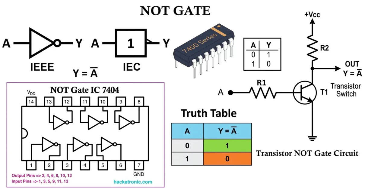
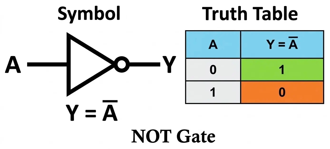
Symbol of NOT Gate
- Standard Symbol (ANSI)
- The most commonly used symbol (ANSI standard) consists of:
- A triangle shape pointing towards the right
- A small circle (inversion bubble) at the output
- One input line entering from the left
- One output line exiting from the right
- The most commonly used symbol (ANSI standard) consists of:
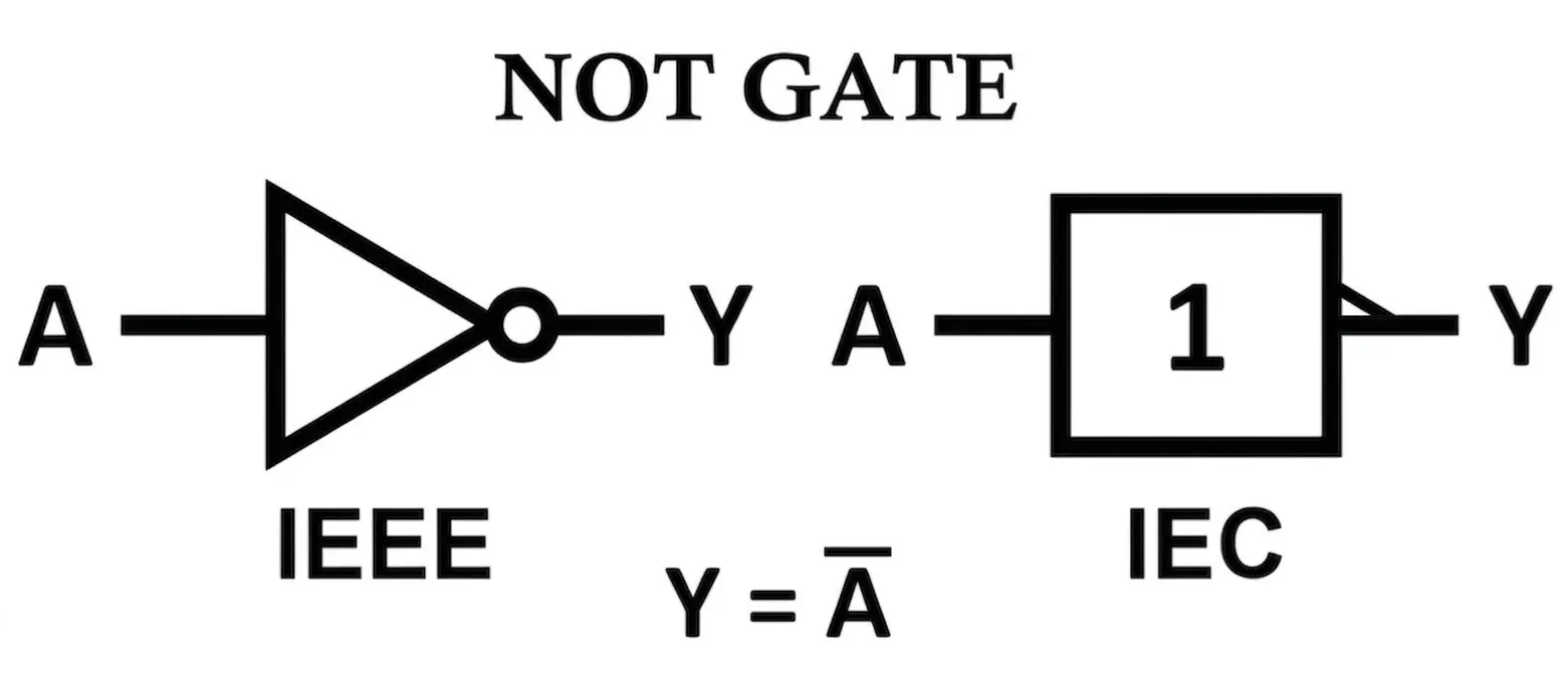
- IEC Symbol
- Represented as a rectangle
- Inside marking: 1 with a small inversion bubble at the output
- Input enters from the left, output exits from the right
- Single-Input Nature
- A NOT gate has only one input (unlike AND/OR gates)
- The logic is fixed: output is always the complement of the input
- Terminal and Notation
- Input: A
- Output: Y or Q
- Boolean expression: Y = A̅ (or Y = ¬A)
- The bar (‾) or symbol (¬) represents the NOT operation (inversion)
- Important Observations
NOT Gate Truth Table
- Working Principle
- The NOT gate operates based on a simple inversion condition:
- Output is HIGH (1) when the input is LOW (0)
- Output is LOW (0) when the input is HIGH (1)
- The NOT gate operates based on a simple inversion condition:
- Unlike OR gates, which evaluate multiple inputs, the NOT gate always produces the complement of a single input.
- Boolean Logic
- The NOT operation follows the Boolean inversion rule: Y = A̅ (or Y = ¬A)
- This is why it is called an inverter gate.
- Key Condition
- Input = HIGH → Output = LOW
- Input = LOW → Output = HIGH
- If A = 1 → Y = 0, If A = 0 → Y = 1
- This makes it extremely useful in signal reversal, control logic, and complement generation.
- Key Observation
- The output is always the opposite of the input
- No multi-input variation exists (unlike OR/AND gates)
- Logic remains fixed: Output = Complement of Input
- It acts as a logical inverter that performs complement generation, not logical combination
NOT Logic Circuit Implementation
The NOT gate (inverter) can be implemented using different hardware technologies. Each implementation has its own characteristics in terms of speed, power consumption, and accuracy.
Transistor NOT Gate (Transistor Inverter Circuit)
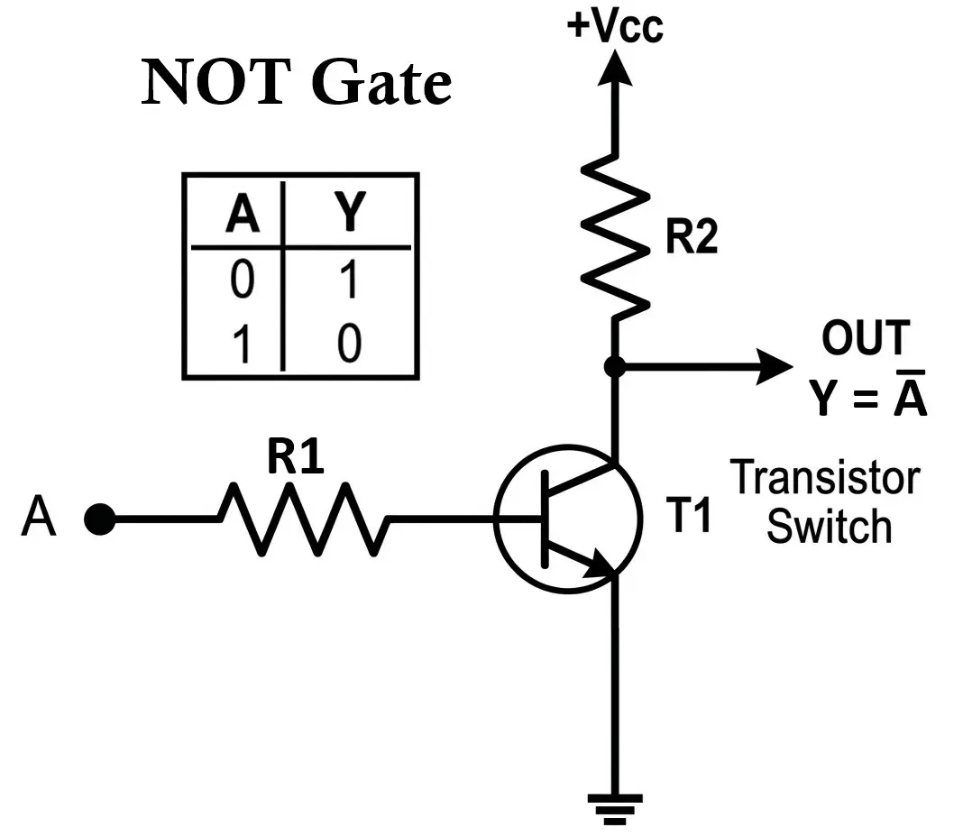
- Working Principle
- Transistor is operated in switching.
- Operation
- Input HIGH (1) → transistor turns ON (saturation) → output becomes LOW (0)
- Input LOW (0) → transistor is OFF (cutoff) → output becomes HIGH (1) via resistor
- Key Insight
- Provides clear inversion using switching behavior
- Widely used in early digital logic families (RTL, TTL)
CMOS NOT Gate (CMOS Inverter Circuit)
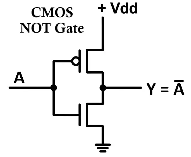
- Structure
- PMOS transistor (pull-up network)
- NMOS transistor (pull-down network)
- Configuration
- PMOS connected to VDD (supply)
- NMOS connected to GND
- Gates tied together as input
- Working
- Input LOW (0): PMOS ON, NMOS OFF → output pulled HIGH (1)
- Input HIGH (1): PMOS OFF, NMOS ON → output pulled LOW (0)
- Advantages
- Very low power consumption
- High noise immunity
- Fast switching speed
- Dominant in modern IC and VLSI design
NAND-Based NOT Gate (NAND as Inverter)
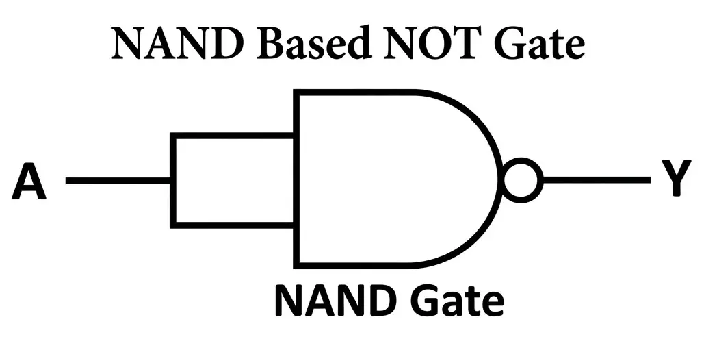
- Boolean Expression: Y = (A · A)̅ = A̅
- Implementation
- Connect both inputs of NAND gate together
- The NAND operation becomes inversion
- Key Insight
- NAND is a universal gate
- An inverter can be implemented using single NAND gate
NOR-Based NOT Gate (NOR as Inverter)
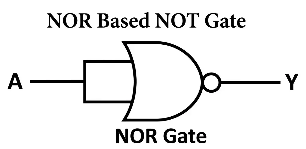
- Boolean Expression: Y = (A + A)̅ = A̅
- Implementation
- Connect both inputs of NOR gate together
- The NOR operation produces inversion
- Key Insight
- NOR is also a universal gate
- Any logic function (including NOT) can be built using only NOR gates
Summary
- NOT is the simplest logic gate, yet essential
- Implemented using diodes, transistors, CMOS, NAND, and NOR
- CMOS inverter is the most widely used practical implementation
- Universal gates (NAND/NOR) allow flexible digital design using minimal gate types
IC Numbers and Details
NOT Gate IC 7404
The 7404 NOT Gate IC is one of the most widely used inverter ICs. It is a Hex Inverter, meaning it contains six independent NOT gates in a single package, belonging to the TTL (Transistor-Transistor Logic) family.
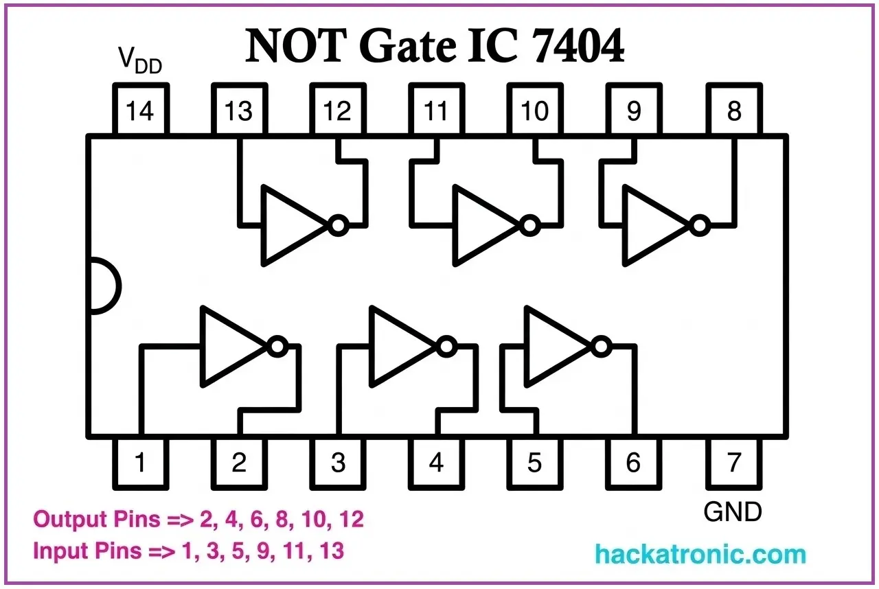
- Features
- Hex inverter (6 NOT gates inside)
- Technology: TTL (BJT-based)
- Propagation delay: ~10 ns
- Power consumption: Moderate (~10 mW per IC)
- Supply voltage: 5V (fixed)
- Fan-out: ~10 TTL loads
- Pin Configuration
- Total pins: 14
- 6 inverters inside IC:
- Gate 1: Input – Pin 1, Output – Pin 2
- Gate 2: Input – Pin 3, Output – Pin 4
- Gate 3: Input – Pin 5, Output – Pin 6
- Gate 4: Input – Pin 9, Output – Pin 8
- Gate 5: Input – Pin 11, Output – Pin 10
- Gate 6: Input – Pin 13, Output – Pin 12
- Power Pins:
- Pin 14: Vcc (+5V)
- Pin 7: GND
Key Characteristic: Each inverter operates independently, allowing multiple signal inversions within a single IC, very useful in compact digital designs and signal conditioning.
74LS04 – Low-Power Schottky TTL NOT Gate
The 74LS04 belongs to the Low-Power Schottky (LS) TTL family, designed to reduce power consumption while maintaining good speed.
- Specifications:
- Technology: TTL with Schottky transistors
- Propagation delay: ~8–10 ns
- Power consumption: Lower than standard TTL
- Supply voltage: 5V (fixed)
- Fan-out: ~10 TTL loads
Key Characteristic: Provides a better speed–power balance, widely used in legacy TTL systems.
74HC04 – High-Speed CMOS NOT Gate
The 74HC04 is part of the High-Speed CMOS (HC) family, offering excellent performance with low power consumption.
- Specifications:
- Technology: CMOS
- Supply voltage: 2V to 6V
- Power consumption: Very low (µW range)
- Propagation delay: ~8–15 ns
- Input impedance: Very high
Key Characteristic: Ideal for modern digital systems, offering high noise immunity and flexible voltage operation.
74HCT04 – TTL-Compatible CMOS NOT Gate
The 74HCT04 is a CMOS inverter designed for TTL compatibility.
- Specifications:
- Technology: CMOS with TTL input compatibility
- Supply voltage: Typically 5V
- Power consumption: Very low
- Propagation delay: Similar to HC series
- Input Levels: LOW ≤ 0.8V, HIGH ≥ 2V
Key Characteristic: Allows direct interfacing between TTL and CMOS circuits without additional level shifting.
CD4069 – CMOS Hex NOT Gate
The CD4069 belongs to the 4000-series CMOS family, known for wide voltage operation and ultra-low power consumption.
- Specifications:
- Technology: CMOS (4000 series)
- Supply voltage: 3V to 15V
- Power consumption: Extremely low
- Propagation delay: ~50–200 ns (voltage dependent)
- Noise immunity: High
Key Characteristic: Best suited for battery-powered and low-frequency applications, where power efficiency is more important than speed.
IC Comparison Table
| IC Number | Technology | Voltage | Speed | Power |
|---|---|---|---|---|
| 7404 | TTL | 5V | Medium | Medium |
| 74LS04 | TTL (LS) | 5V | High | Low |
| 74HC04 | CMOS | 2–6V | High | Very Low |
| 74HCT04 | CMOS + TTL | 5V | High | Low |
| CD4069 | CMOS | 3–15V | Medium | Very Low |
- 7404 series ICs are the standard choice for NOT gate implementation
- CMOS versions (74HC04, CD4069) dominate modern electronics due to low power consumption
- TTL variants (7404, 74LS04) are still used in educational and legacy systems
- Multiple inverters in a single IC improve design efficiency and compactness
Timing and Practical Considerations
- Propagation Delay
- Time taken for the output to respond to a change in input
- TTL NOT gates (7404): ~10 ns
- CMOS NOT gates (74HC04): ~8–15 ns (can be lower in advanced ICs)
- Critical in high-frequency circuits, clock signals, and digital timing systems
- Fan-In and Fan-Out
- Fan-In: NOT gate has only one input → fan-in is fixed
- Fan-Out: Number of inputs a logic gate output can drive
- TTL: ~10 loads
- CMOS: Much higher due to high input impedance
- Noise Margin
- CMOS > TTL
- CMOS gates provide better noise immunity
- Important for stable operation in noisy environments, industrial systems, and embedded designs
- Power Consumption
- TTL: Higher power consumption
- CMOS: Extremely low (µW range)
- NOT gates implemented in CMOS are preferred for:
- Battery-powered devices
- Portable electronics
- Low-power embedded systems
NOT Logic Example
- Signal Inversion
- Consider a system with one condition:
- Enable signal (A)
- Output (Y) = Disabled system
- The system is designed such that:
- When input is HIGH → system is OFF
- When input is LOW → system is ON
| A | Y = A̅ |
|---|---|
| 0 | 1 |
| 1 | 0 |
This gate is used to reverse control logic.
NOT Logic Circuit Implementations
- Using Switches (Mechanical Logic)
- A single switch with inverted wiring logic
- Open switch → Output HIGH
- Closed switch → Output LOW
- Used in: Reset circuits, interrupt systems, safety shutdown mechanisms and basic electrical control systems
- Using Relay Logic
- Relay configured for normally closed (NC) operation
- When input energizes relay → output disconnects
- When input is OFF → output remains active
- Used in: Industrial control panels and safety interlock systems
- Using FPGA / Digital Systems
- Implemented using HDL: assign Y = ~A;
- Used in: FPGA design, ASIC development, and digital signal processing systems
Applications
- Logic and Signal Processing
- Signal inversion
- Complement generation
- Boolean logic simplification
- Karnaugh Map (K-map) optimization
- In Digital Electronics
- Adders and subtractors (complement operations)
- Flip-flops and memory circuits
- Counters and registers
- Control logic circuits
- In Computing Systems
- CPU control signals
- Instruction decoding
- Memory addressing logic
- Active-low signal design
- In Everyday Electronics
- Reset circuits
- Inverter-based oscillators
- LED control (active-low logic)
- Safety shutdown systems
Advantages
- Extremely simple and easy to implement
- Essential for logic inversion and complement generation
- Fast switching capability
- Low cost and widely available
- Crucial for building complex logic systems
Limitations
- Works on only one input
- Cannot perform decision-making alone
- Always requires combination with other gates
- Limited functionality in isolation
NOT Gate vs AND Gate vs OR Gate
| Feature | NOT Gate | AND Gate | OR Gate |
|---|---|---|---|
| Boolean Expression | A̅ | A · B | A + B |
| Output Condition | Inverts input | All inputs HIGH | Any input HIGH |
| Output Behavior | Opposite | Strict | Flexible |
- Key Differences:
- NOT Gate: Reverses the input logic
- AND Gate: Requires all conditions to be true
- OR Gate: Requires at least one condition to be true
Conclusion
The NOT gate is the simplest yet one of the most essential components in digital electronics. It performs logical inversion, producing an output that is always the complement of its input.
Key Insights
- NOT logic gate is a fundamental inverter element
- Used in:
- Signal inversion
- Control logic
- Active-low system design
- Symbol identified by triangle with inversion bubble
- Truth table defines complementary behavior
- Implemented using:
- Transistors
- CMOS technology
- Universal gates (NAND/NOR)
- Available in IC families:
- 7404, 74LS04, 74HC04, CD4069
From simple signal inversion to complex digital systems, the NOT gate plays a critical role in enabling logical operations and system control. A strong understanding of the NOT gate is essential for mastering digital electronics and circuit design.
Types of Logic Gates with Symbol, Truth Table and IC Numbers
AND Gate: Symbol, Truth Table, Logic Circuit, and IC Numbers
Universal NAND Gate Truth Table, Logic Circuit & IC 7400 Pin Diagram
Universal NOR Gate Truth Table, Logic Circuit & IC 7402 PIN Diagram
