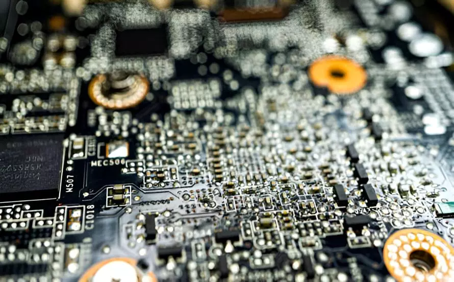
In this article you will learn about High Density Interconnect HDI PCB. The basic definition, how it differs from simple PCBs, and the benefits of high-density interconnect boards. We will explore the application areas and understand the importance of PCB in this category.
We are living in the era of miniaturization. Every person living on the Earth is surrounded by a minimum of 3 to 4 electronic devices around them. Mobile phones, laptops, Wireless chargers, tablets etc. are abundant. The Engineers are constantly innovating, redesigning and reducing the size and weight of complete products to match the competitors. Printed circuit boards have also evolved to support complex product design and development.
What is HDI PCB?
HDI is the abbreviation for High Density Interconnect. It functions similarly to simple PCB, but HDI PCB boards are fabricated with more layers and different PCB substrate materials. IPC-2226 standard defines the boards that have large wiring density per unit area when compared to simple boards The electrical performance supports high speed, high frequency, RF signals and complex circuitry. These boards make use of micro vias, blind and buried vias. The layer stackup must be defined properly to achieve a fast response in the HDI circuit. The number of surface mount component counts, high power requirements, signal integrity, the limited board size, and a couple of differential pairs are the few features of high-density boards. This kind of PCB is relatively hard to fabricate so we need reliable printed circuit board manufacturers to realize the ideal HDI PCBs.
Features of High-Density Interconnect PCB Board
These boards incorporate many parts in a small space. They have more advantages and benefits than traditional PCBs. Let us learn about the special features of HDI PCB boards.
- High-density boards are smaller in size.
- HDI PCB boards have less weight.
- High-density boards provide improved signal integrity.
- High-density boards use thin trace-width.
- HDI PCB boards have better board performance.
- High-density boards take less time to manufacture.
- High-density boards are reliable for longer times.
- HDI PCB boards are cost-effective.
- High-density boards are built in compact shapes and sizes.
- High-density boards use different via types of filling (plugged, filled, capped, metallized and tented)
- High-density boards are designed as multi-layers from 4,6,8,10,12 etc.
Types of Via Styles in HDI Board
HDI PCB boards employ more connections amongst board elements than regular circuit boards. Via is essential to make electrical connections between layers. The structure of via in the layer stackup has many ways. It is defined by IPC standards. We will learn about them in detail below.
Through-Hole Vias
A hole is drilled in the PCB. This hole can be plated or non-plated. Plated means the hole has a copper outline for electrical conductivity. Through-hole vias provide a connection from the top layer to the bottom layer. All the inner layers are also drilled. Drilling through holes in HDI PCBs is easy and cost friendly.
Microvia
It is the smaller version of through hole via. The diameter of microvias is less than 120 microns. The drilling is done using laser technology, which provides a connection from any one layer to the next layer. These are widely used in HDI PCB boards. Due to microvias, it is possible to have a high density of components in small areas.
Blind Microvia
Blind via are named as blind because the via starts from the outer layer and ends in one inner layer. It is widely used in the HDI PCB fabrication. The electrical connection is not available throughout the top-to-bottom layer. Blind vias are laminated.
Buried Microvia
Buried microvia cannot be seen from outside the PCB layer top or bottom. The via is drilled to connect any two inner layers. They have the advantage over blind vias as they provide space on the layers for routing traces. It is another hole commonly used in the HDI PCB. The diameter of it is less than 7 mils.
Skip Via
As the name says skip, the skip via will skip one layer in the stackup. The conductivity is possible in the skipped layer. But this kind of vias is difficult to drill in the HDI PCB.
Stacked Via
The vias are stacked on each other making a stack. Copper is filled in these vias.
Staggered Via
Staggered vias are not stacked on top of each other. They are in different positions on each layer. They take less time to fabricate because copper filling is not required.
Type I
It has microvia embedded in the PCB core. The type 1 structure uses plated microvia or PTH on one side or both sides of the stackup. The microvia is blind and connects from either the top layer or bottom layer on one side. The layer stackup is called 1+n+1 because the layer of microvia used is a single
Type II
This type 2 structure also uses a single layer of microvia in the PCB core. It is similar to Type 1. The advantage of using blind vias and buried vias is available in type 2 via styles.
Type III
The microvia layers are at least 2 for each side of the stackup. The vias are plated. Both the blind and buried vias are used. The layer stackup is called 2+n+2 because the layer of microvia used is double.
Importance of High-Density Interconnect HDI PCB Boards
Designers have the option to work on any type of PCB like single-layer, or multi-layered. Choose any PCB material, and surface finish to assemble it. Based on the product requirement that mentions high-speed communication protocols like USB, HDMI, PCIe, and Ethernet. Engineers have to work with HDI PCB boards. We will explore the importance and advantages of high-density boards.

Less Space with More Density
A complex circuit has many sections that operate on mixed signals. We have to add various integrated chips for the power supply, communication, analog section, and microcontroller. Each section requires many components. The HDI type of PCB is used to place more parts in limited space.
No Signal Reflection
In high-speed communication protocols. signal reflection, signal loss is a major issue that must be catered. Working on a normal PCB will not solve this problem. In HDI PCB boards, parts are placed in proximity, reducing the trace length and noise generation is optimized.
The Number of Layers is Reduced
The special feature of HDI PCB boards is compactness. When we use normal boards with through hole components and vias, we must add more layers to fit all the parts. Microvias allow extra space on the outer layers for component placement. This will lower the layer count for signal routing. The cost linked to board manufacturing is also optimized.
The Boards Built are Reliable
With no signal noise, or EMI interference. A HDI PCB board created reliable boards that are suitable for harsh environments. Make sure all the compliance tests are also performed that provide quality boards. No repairs and faults will improve the board’s lifetime.
Suitable for Various Product Requirements
Less space, high signal strength, high speed, high frequency, less weight, and improved electrical performance are some of the specifications of product development. HDI PCB board is fitted in all aspects of electronic devices.
Summary
Any printed circuit manufacturer who has previous experience in fabricating High-Density Interconnect (HDI) PCB, and RF PCB can deliver high-quality boards. Considering the versatile application areas such as Medical, automotive, consumer electronics, aerospace, communication devices and computers of high-density boards. It is important for printed circuit board manufacturers to accomplish high-quality board performance.
Revolutionary Axial Flux Printed Circuit Board (PCB) Stator Motor
Gold Finger PCB Assembly: Best Practices for Ensuring Reliability


