In this article, you will learn how to design a 12V 5A SMPS circuit that converts 230VAC to regulated 12V DC using the TOP227YN in a flyback configuration.
Switched Mode Power Supplies (SMPS) are widely used for high-efficiency AC-to-DC conversion. The flyback topology is especially suitable for low- to medium-power isolated supplies. The TOP227YN is a highly integrated offline switcher IC with an internal high-voltage MOSFET and protection features, making it ideal for compact 60W designs.
We will also cover transformer design, turns ratio calculations, and practical implementation details.
SMPS Specifications
Before starting the design, let’s summarize the specifications of this 12V power supply:
- Input Voltage: 230V AC (rectified to ≈ 325V DC)
- Output Voltage: 12V DC (adjustable ±5%)
- Output Current: 5A
- Output Power: 60W
- Topology: Isolated Flyback
- Controller IC: TOP227YN (Integrated 700V MOSFET)
- Switching Frequency: 100 kHz
- Control Mode: Current Mode PWM
- Isolation: Transformer + Optocoupler
- Efficiency: Typical efficiency: 75–85%
- Efficiency depends on:
- Transformer design
- Schottky diode selection
- Output capacitor ESR
- Switching frequency
- Efficiency depends on:
This design targets moderate power applications such as LED systems, embedded electronics, and communication devices.
Overview of TOP227YN Controller
The core of the circuit is TOP227YN, an integrated off-line PWM switcher from the TOPSwitch-II family. Key features include:
- Integrated high-voltage MOSFET
- Internal oscillator and current-mode control
- Thermal shutdown
- Overcurrent protection
- Auto-restart fault protection
- Minimal external components required
It simplifies the flyback converter design by integrating the control circuitry and power switch inside one TO-220 package.
Related Articles:
- 12V 10A SMPS: Switched Mode Power Supply Circuit – IC DM0565
- Switch Mode Power Supply SMPS Block Diagram & Working
- Flyback Converter vs Forward Converter – Detailed Comparison
What is Flyback Topology?
- In a flyback converter:
- When the internal MOSFET (inside TOP227YN) turns ON, energy is stored in the transformer core.
- When it turns OFF, stored energy is transferred to the secondary and delivered to the load.
- Advantages:
- Provides galvanic isolation
- Requires fewer components
- Ideal for power levels below 100W
- Cost-effective for compact designs
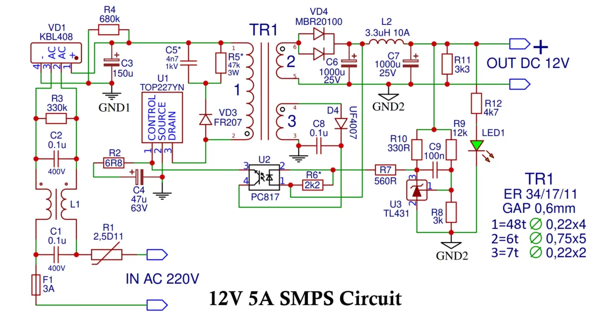
IC TOP227YN 12V 5A SMPS Circuit Diagram
The circuit can be divided into five major sections:
- Input EMI & Rectification Stage
- Primary Switching Stage
- Flyback Transformer
- Secondary Rectification & Filtering
- Feedback & Regulation Network
Input Section (AC 220V to DC Bus)
Components Involved
- F1 – 3A Fuse
- R1 – NTC Thermistor (2.5D11)
- C1, C2 – 0.1µF EMI Capacitors
- L1 – Common Mode Choke
- VD1 – KBL408 Bridge Rectifier
- C3 – 150µF / 400V Bulk Capacitor
- R3, R4 – Bleeder Resistors
Working
- Fuse (F1) protects against catastrophic short circuits.
- NTC thermistor (R1) limits inrush current during startup.
- EMI filter (C1, C2, L1) suppresses conducted noise.
- Bridge rectifier (KBL408) converts 220VAC into high voltage DC.
- C3 smooths the rectified DC to approximately:
VDC ≈ 220 × 1.414 ≈ 310V DC
This 310V DC becomes the input for the flyback converter.
Primary Switching Stage
Components
- U1 – TOP227YN
- R2 – 6.8Ω (Source resistor)
- C4 – 47µF (Control bypass capacitor)
- R5, C5, VD3 – Snubber Network
Working Explanation
This circuit operates in discontinuous or boundary conduction flyback mode under typical load conditions. TOP227YN operates in current-mode flyback topology. Let’s See Switching Cycle Operation:
Stage 1 – MOSFET ON (Energy Storage Mode)
When the internal MOSFET of TOP227YN turns ON:
- Primary current rises linearly.
- Secondary diode (MBR20100) is reverse biased.
- Energy is stored in transformer magnetizing inductance.
Primary current slope:
di/dt = Vin / Lp
Where: Vin ≈ 310V, Lp = Primary inductance
Stage 2 – MOSFET OFF (Energy Transfer Mode)
When MOSFET turns OFF:
- Primary current drops instantly to zero.
- Secondary diode becomes forward biased.
- Stored energy transfers to output.
Peak drain voltage:
VDS(max) = Vin + (Np/Ns)(Vout + Vd) + Vspike
Snubber Network
- R5 (47kΩ, 3W)
- C5 (4.7nF, 1kV)
- VD3 (FR207)
This RCD snubber absorbs voltage spikes caused by transformer leakage inductance and protects the internal MOSFET.
Flyback Transformer (TR1) Design Calculations
The transformer is the most critical component in a flyback SMPS. For this
12V / 5A (60W) power supply using the TOP227YN and ER34/17/11 ferrite core,
the transformer must be designed considering low-line operation, maximum
duty cycle, and safe flux density.
Design specifications:
- Input voltage (after rectification): 255V–325V DC
- Output voltage: 12V DC
- Output current: 5A
- Switching frequency: ≈100kHz
- Target maximum flux density (Bmax): 0.20 Tesla
- Ferrite Core: ER34/17/11, Air Gap: 0.6mm
- Effective core area (Ae): 125 mm²
Turns Ratio Calculation (Flyback Topology)
For a flyback converter, the turns ratio is determined using reflected voltage
rather than the simple Vin/Vout ratio used in forward converters.
We choose a reflected voltage of approximately 100V for good efficiency and
safe MOSFET stress.
Reflected voltage formula:
Np/Ns = Vreflected / (Vout + Vd)
Where: Vout = 12V, Vd ≈ 0.5V (Schottky diode drop)
Np/Ns = 100 / 12.5 = 8
Therefore, the primary-to-secondary turns ratio is approximately:
Np:Ns = 8:1
Primary Turns Calculation
Primary turns are calculated using the volt-second balance equation:
Np = (Vin(min) × Dmax) / (Bmax × Ae × f)
Where: Vin(min) = 255V, Dmax = 0.45, Bmax = 0.20T, Ae = 125 × 10-6 m², f = 100kHz
Substituting:
Np = (255 × 0.45) / (0.20 × 125 × 10-6 × 100000)
Np ≈ 46 turns
For design margin and ease of winding, we round up:
Primary Turns (Np) = 48 turns
Secondary Turns Calculation
Using the turns ratio of 8:1:
Ns = Np / 8
Ns = 48 / 8 = 6
Secondary Turns (Ns) = 6 turns
Auxiliary Winding Calculation
The auxiliary winding provides Vcc (~15V) for the TOP227YN.
Naux = (Vaux / (Vout + Vd)) × Ns
Where: Vaux ≈ 15V, Vout + Vd = 12.5V
Naux = (15.7 / 12.5) × 6
Naux ≈ 7.5
Auxiliary Turns = 7 turns
Final Transformer Winding Data
- Primary winding: 48 turns
- Secondary winding: 6 turns
- Auxiliary winding: 7 turns
- Air gap: approximately 0.5–0.7 mm (adjusted to achieve correct primary inductance)
Voltage Stress Verification
Reflected voltage:
Vreflected = 12.5 × 8 = 100V
Maximum MOSFET voltage stress at high line (325V DC):
VDS(max) = 325 + 100 = 425V
This is well within the 700V rating of the TOP227YN internal MOSFET,
ensuring safe and efficient operation.
This transformer configuration provides:
- Proper duty cycle margin
- Controlled flux density
- Reduced switching stress
- Improved efficiency
- Reliable regulation under low-line conditions
The above calculations ensure the ER34/17/11 core is optimally designed
for a stable 12V, 5A flyback SMPS.
Secondary Rectification, Output Filter and Auxiliary Supply
Components
- VD4 – MBR20100 (Schottky Diode)
- L2 – 3.3µH, 10A Inductor
- C6, C7 – 1000µF / 25V Electrolytic Capacitors
- D4 – UF4007
- C8 – 0.1µF
Operation
- When the primary switch turns OFF:
- Secondary voltage becomes forward biased.
- MBR20100 rectifies the pulse waveform.
- Inductor L2 and capacitors form an LC filter.
- Output becomes stable 12V DC.
- Schottky diode is selected because:
- Low forward voltage drops
- Fast switching
- High efficiency at 5A load
Auxiliary winding supplies power to the control circuitry after startup, improving efficiency by eliminating continuous startup resistor dissipation.
Feedback and Voltage Regulation
Components
- U3 – TL431 (Adjustable Shunt Regulator)
- U2 – PC817 (Optocoupler)
- R6–R7–R10 – Feedback Network
- C9 – Compensation Capacitor
Working
- Output voltage is sampled via resistor divider (R8, R9).
- When output exceeds 12V:
- TL431 conducts.
- LED inside PC817 turns ON.
- Optocoupler transistor pulls feedback pin of TOP227YN.
- PWM duty cycle reduces.
- Output voltage stabilizes.
- This provides:
- Electrical isolation
- Accurate voltage regulation
- Stable control loop
Output Indicator
- LED1 with R12 indicates output presence.
- R11 acts as minimum load/bleeder.
Feedback Loop Compensation Analysis
Control architecture:
- TL431 → Error amplifier
- PC817 → Isolation
- TOP227 → PWM controller
TL431 Reference
Internal reference = 2.5V
Vout = 2.5 × (1 + R9/R8)
Given: R8 = 3kΩ, R9 = 12kΩ
Vout = 12.5V
Compensation Network
R10 + C9 form Type-II compensation to:
- Cancel output pole
- Improve phase margin
- Prevent oscillation
fp = 1/(2π Rload Cout)
For Rload = 2.4Ω and Cout ≈ 2000µF: fp ≈ 33Hz
PCB Layout Guidelines for SMPS
- High di/dt Loops
- MOSFET → Primary winding → Bulk cap → MOSFET
- Very short traces
- Thick copper
- Minimal loop area
- Separate Grounds
- Primary GND
- Secondary GND
- Isolate via optocoupler only
- Snubber Placement
- Place RCD snubber close to transformer and IC
- Minimize trace inductance
- Output Section
- Schottky diode near transformer
- Tight LC filter layout
- Wide copper for 5A output
- Creepage & Clearance
- 6–8mm minimum isolation gap for 220VAC
- Transformer slot cut recommended
- Thermal Considerations
- Heatsink for TOP227YN
- Heatsink for MBR20100
- Ensure airflow clearance
Efficiency Optimization Tips
- Low ESR Output Capacitor
- Reduce ripple and power loss.
- Proper Schottky Diode Selection: P = I × V = 5A × 0.5V = 2.5W
- Optimize Transformer Design
- Reduce leakage inductance
- Tight winding coupling
- Proper insulation layers
- Reduce Snubber Loss
- Optimize R and C values to reduce heating.
- Minimize Switching Loss
- Lower peak current reduces MOSFET stress and improves efficiency.
Thermal Management
Although 60W is moderate power, heat dissipation must be considered.
- Use a small heatsink for TOP227YN
- Provide airflow
- Use wide PCB traces for secondary current paths
- Keep primary and secondary grounds separated
Efficiency typically ranges between 80–85% for a properly designed flyback.
Protection Features
This design includes:
- Internal protections (TOP227YN):
- Cycle-by-cycle current limiting
- Thermal shutdown
- Auto-restart
- Line undervoltage detection
- External protections:
- MOV for surge suppression
- NTC for inrush limiting
- Input fuse
- RCD snubber for MOSFET protection
Simulation and Testing
- Before hardware implementation:
- Simulate in LTspice or similar
- Verify drain voltage waveform
- Ensure no excessive overshoot
- Confirm output ripple < 100mV
- After building:
- Measure no-load voltage
- Check full-load current (5A)
- Monitor temperature of IC, diode, transformer
- Verify regulation from 180VAC–260VAC
Advantages of Flyback Design
- High efficiency compared to linear power supplies
- Compact and lightweight design (high-frequency operation)
- Wide input voltage range support (255–325V DC)
- Simple topology with low component count
- Built-in protection features in TOP227YN (OCP, OVP, thermal shutdown)
- Good isolation between primary and secondary
- Suitable for low-to-medium power (≈60W) applications
- Cost-effective transformer and control implementation
- Stable 12V output regulation under varying line conditions
- Reliable operation in DCM/Boundary mode
Disadvantages of Flyback SMPS
- High peak current stress in DCM operation
- MOSFET voltage spikes due to leakage inductance
- EMI generation from high-frequency switching
- Higher output ripple compared to forward/LLC converters
- Output diode thermal stress
- Snubber power loss reduces efficiency
- Light-load efficiency is lower
- Requires careful transformer design and PCB layout
- Thermal management needed for 60W compact design
- Not ideal for scaling to higher power levels (>100W)
Applications of 12V 5A SMPS Circuit
A 12V 5A SMPS (60W) is widely used in:
- LED Lighting Systems – Powers LED strips and fixtures with high efficiency, stable voltage, and low heat for longer LED lifespan and consistent brightness.
- Telecommunication Equipment – Supplies regulated 12V to modems, routers, and communication systems requiring compact, reliable, low-heat power solutions.
- Battery Chargers – Provides controlled voltage and current for safe charging of 12V lead-acid, Li-ion, and other rechargeable batteries.
- Embedded Systems – Delivers clean and stable DC power to microcontrollers, sensors, and control electronics, minimizing electrical noise.
- Consumer Electronics – Used in TVs, audio systems, gaming consoles, and media devices requiring efficient AC-to-DC conversion.
- CCTV and Security Systems – Ensures continuous and stable operation of cameras, DVRs, and surveillance equipment with surge tolerance.
- Automotive Accessories – Powers car audio systems, GPS units, and LED lighting while maintaining stable output despite input voltage variations.
- Industrial Control Systems – Supplies reliable 12V DC to PLC panels, relays, actuators, and automation equipment in demanding environments.
- Medical Equipment – Provides precise and low-noise power for diagnostic devices, monitoring systems, and portable medical instruments.
- Portable Devices – Supports battery packs, portable amplifiers, and mobile electronics where efficiency and compactness are critical.
- Audio Amplifiers – Supplies clean and regulated 12V DC to minimize distortion in low- and medium-power audio systems.
- Home Appliances – Used in low-voltage household electronics such as cordless phones, clocks, and automation systems.
- Robotics and Drones – Provides lightweight, efficient, and stable power to motors, controllers, and onboard electronics.
- Arduino and Raspberry Pi Systems – Powers development boards and IoT prototypes requiring regulated 12V DC input.
- Solar Power Systems – Converts variable solar panel output into stable 12V DC for off-grid and renewable applications.
- Test and Measurement Equipment – Supplies precise and stable DC power to oscilloscopes, multimeters, and laboratory instruments.
Its compact size and high efficiency make it suitable for continuous operation devices.
Conclusion
The 12V 5A SMPS using TOP227YN is a robust and efficient flyback converter suitable for medium power applications around 60W. The integration of high-voltage MOSFET and PWM controller inside TOP227YN significantly reduces component count and design complexity.
- This 60W implementation:
- Uses a smaller transformer core
- Requires lower current rating components
- Produces less thermal stress
- Offers easier PCB layout
By carefully selecting the transformer turns ratio, core material, snubber network, and feedback components, you can build a reliable and robust 12V 5A isolated power supply.
12V 10A SMPS: Switched Mode Power Supply Circuit – IC DM0565
Flyback Converter vs Forward Converter – Detailed Comparison
H Bridge Inverter Circuit using IC SG3525 and MOSFET IRFZ44N
