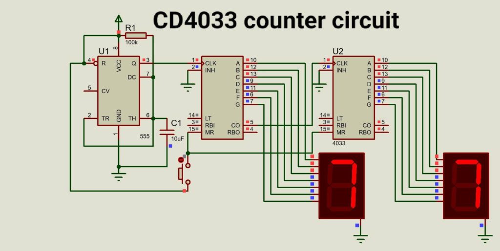
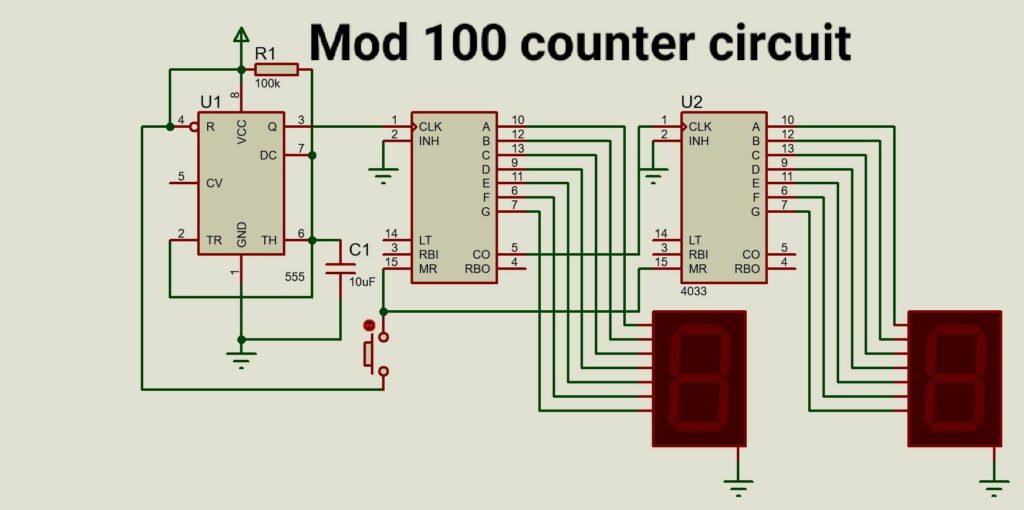
In this project, we will be making CD4033 counter circuit. a mod-100 counter circuit (0 to 99). We are using a 555 timer, CD4033 counter 7 segment display, and some other components. It is a very simple counter circuit. Counter circuits are often used to count objects, people, and many other things.
Components required:
- 555 timer – 1
- CD4033 counter IC – 2
- Seven segment display (common cathode) – 2
- Push-button – 1
- 10uf Capacitor – 1
- 100k resistor – 1
- 5V power supply
Circuit explanation:
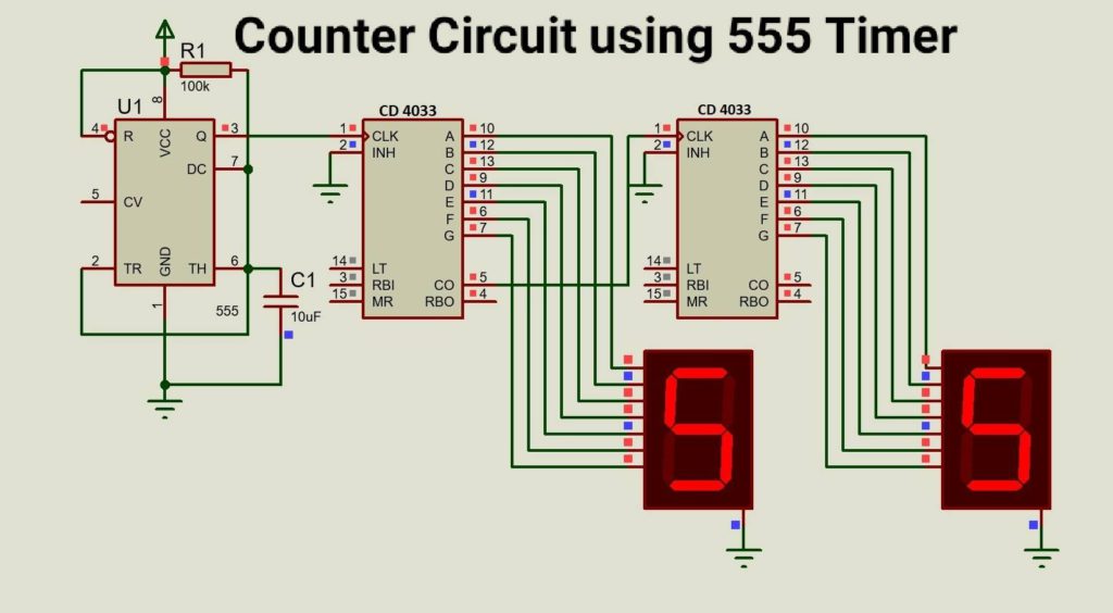
In the 555 timer pin 2,6 and 7 are shorted and connected to the capacitor C1. pin 4 and 8 are connected to Vcc. pin 3 is the output pin. In the case of CD4033 IC pin 1 is the clock input. pin 15 is the reset pin, by applying +Vcc you can reset the count to 0. PIN 6,7,9,10,11,12,13 are given to the seven-segment display.
555 timer working:
We are using 555 timer in astable multivibrator mode. In this mode, it generates clock pulse of desired frequency.
You can use it in monostable mode to manually give clock pulse.
CD4033 counter for 7 segment display:
CD4033 is a counter for 7 segment display. If we use counter ic like 7490, you can make a 7490 decade counter circuit but we have to use a separate seven-segment decoder IC LM7447 seven-segment decoder IC which will increase the cost and complexity. That’s why we are using CD4033 IC, it is easy to use.
Seven Segment Display:
To count from 0 to 99 we need two seven-segment displays. Both are common cathode displays.
know opamp’s basic concept hackatronic.com
Working of Counter Circuit using 555 timer:
For the counter to count it needs clock pulses. The 555 timer is working in astable multivibrator mode, It generates clock pulses.
The output of the first counter is given to seven-segment display. It gives the least significant bit LSB of count. The final carry is given as output to the next IC as input clock. This IC gives count for MSB ( maximum significant bit).
While counting if you want to reset the circuit press the reset button. It will make the count 00.
This is how the CD4033 counter circuit using 555 timer works.


Very very useful for my project
Your project is nice and useful, I have a question, can you please publish up down counter by this IC cd 4033 ?
sure
I ordered uxcell Common Cathode 10 Pin 1 Bit 7 Segment to use as my numeric segments. These have 5 pins on the top of the segment, and 5 pins on the bottom of the segment. I see that the pins used on cd4033 are 10, 12, 13,9, 11, 6, 7 with pin 5 sending a clock pulse to pin 1 of the 2 cd4033 ic’s. My question is: what pins on the segments are used with 10, 12, 13,9, 11, 6, 7? There are 5 on the top, and 5 on the bottom. Can you tell me? Great’ly appreciate it The very bottom of both segments are grounds. A pinout of my segments would save my life. I’d owe you a HUGE favor.
It’s a general 7 segment display you can find it’s pinot on google. if you have part number try searching it.
https://www.youtube.com/watch?v=OkGV0TTTlrc
The gentleman in the above video explains the 7 Segment and the 4033 pin out’s quite well. I’ll post this to aid anyone needing and questions answered.
I’m still a huge fan of yours, though. Love your work with the 555. Although many will cite Forest Mim’s as predating this work, your stuff demonstrates real experience working with the 555.
Keep up the great work, sir!
Thank You
Another thought:
The 74 hundred line can, at times, be difficult to obtain.
Be advised: the 54 hundred line is electrically the same as the 74 hundred device by device, with one difference: the 54 hundred line are a military line: the same as the 74 hundred, but beefier.
Example: the 74LS221 is a dual, monostable, multivibrator. The 54LS221 is too, but the 54LS221 is the better choice. Its temp rating is superior, as it’s a military chip.
Just a little something I learned in the 1970’s, that’s good to know.
Can you make it count minus? 99 to 0 also ?
Try CD40110 IC