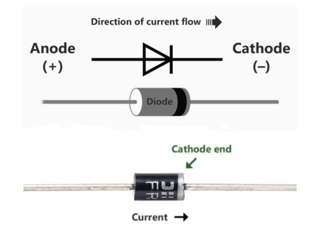
The definition of diode is very simple, “A diode is a two-terminal polarized electronic component which mainly conducts current in one direction and blocks in other direction”. Its resistance in one direction is low (ideally zero) and high (ideally infinite) resistance in the other direction. There are various types of Diodes like Zener, Schottky, tunnel, varactor, etc.. you must read this article Types of diode and symbol of Diode.
PN Junction Diode Explained:
1.) A diodes show’s such special behavior due to the junction formed between the two (N-type and P-type) materials used to construct it.
2.) N-type material has electrons as majority Carrier and holes as minority carriers. Whereas type material has holes as majority Carrier and electrons as minority carriers.
2.) An ideal Diode has two terminals anode (+) and cathode (-) when the positive terminal of a battery is connected to the anode and -ve terminal to cathode the diode conducts current, here the diode is said to be in forward bias mode, where it acts as a good conductor.
Symbol of Diode in forward bias:
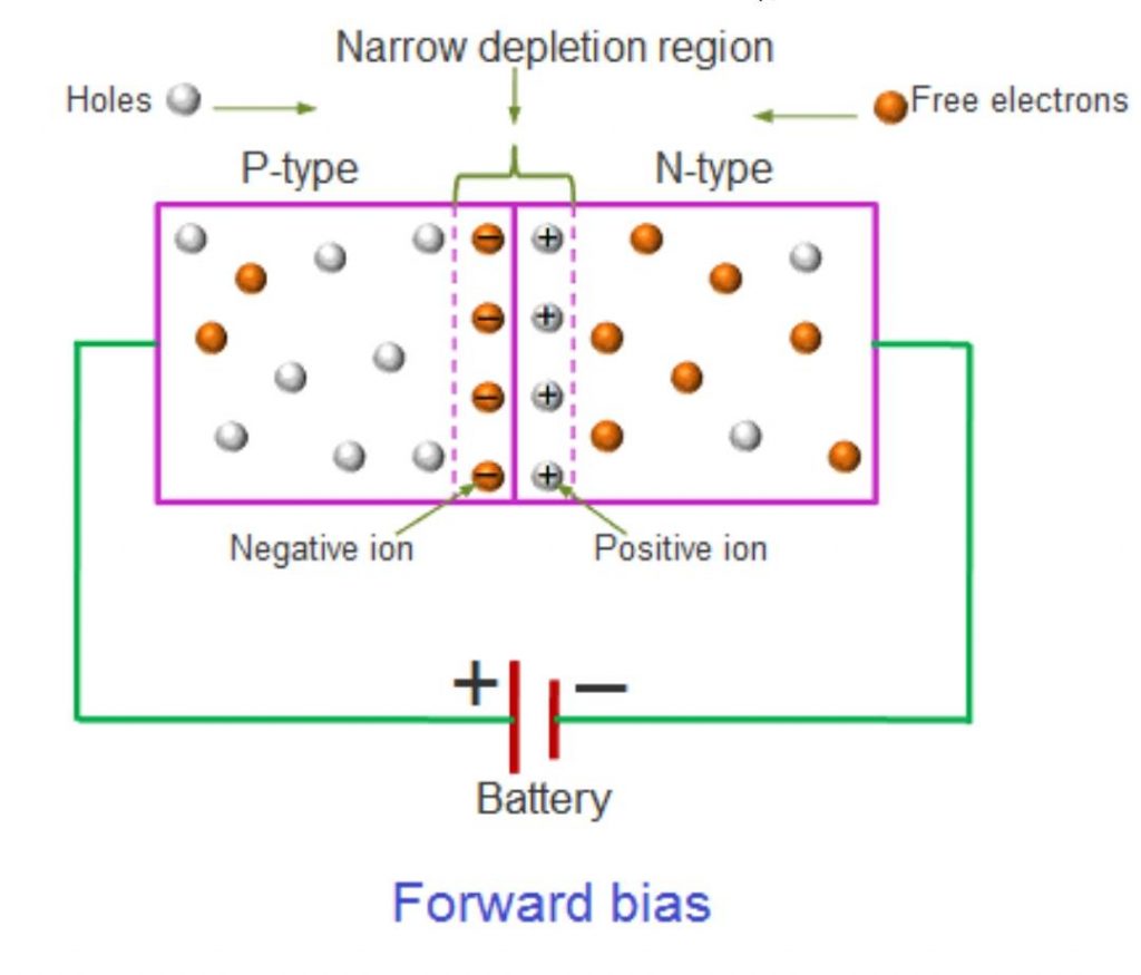
3.) But practically its behavior is slightly different from the ideal condition. In the forward direction, it conducts after a certain value of Voltage applied across it known as knee Voltage or barrier voltage or forward Voltage. This happens due to the presence of a depletion layer between two materials. This depletion region forms due to the recombination of holes and electrons near the junction. After crossing knee Voltage current through the diode starts increasing rapidly and the depletion region vanishes.
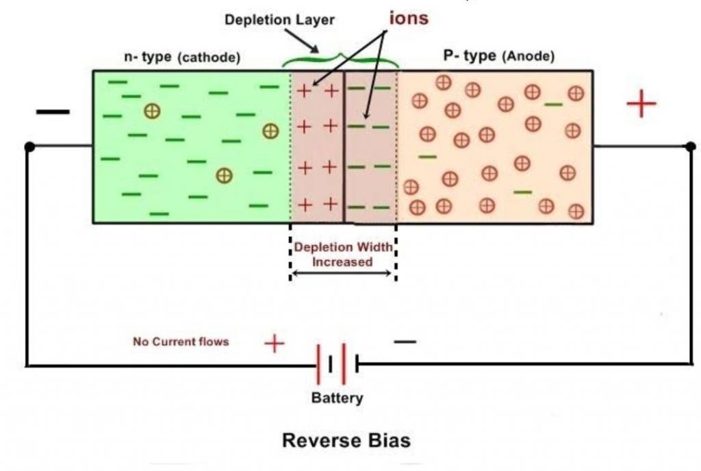
3.) When the diode is reverse biased means its anode is connected to -ve and cathode is connected to +ve of battery it offers very high resistance and doesn’t conduct current in the reverse direction.
5.) In reverse direction as the voltage is applied across the diode, the width of the depletion region between the two N and P-type materials starts increasing and Diode doesn’t Conduct. This happens due to the recombination of electronics and holes from both sides of the junction. But practically it conducts current in a very small quantity in order of few nano-ampers to micro-ampers ) due to the presence of minority carriers on both sides of the junction.
As shown in the figure
The V-I characteristics of PN Junction Diode:
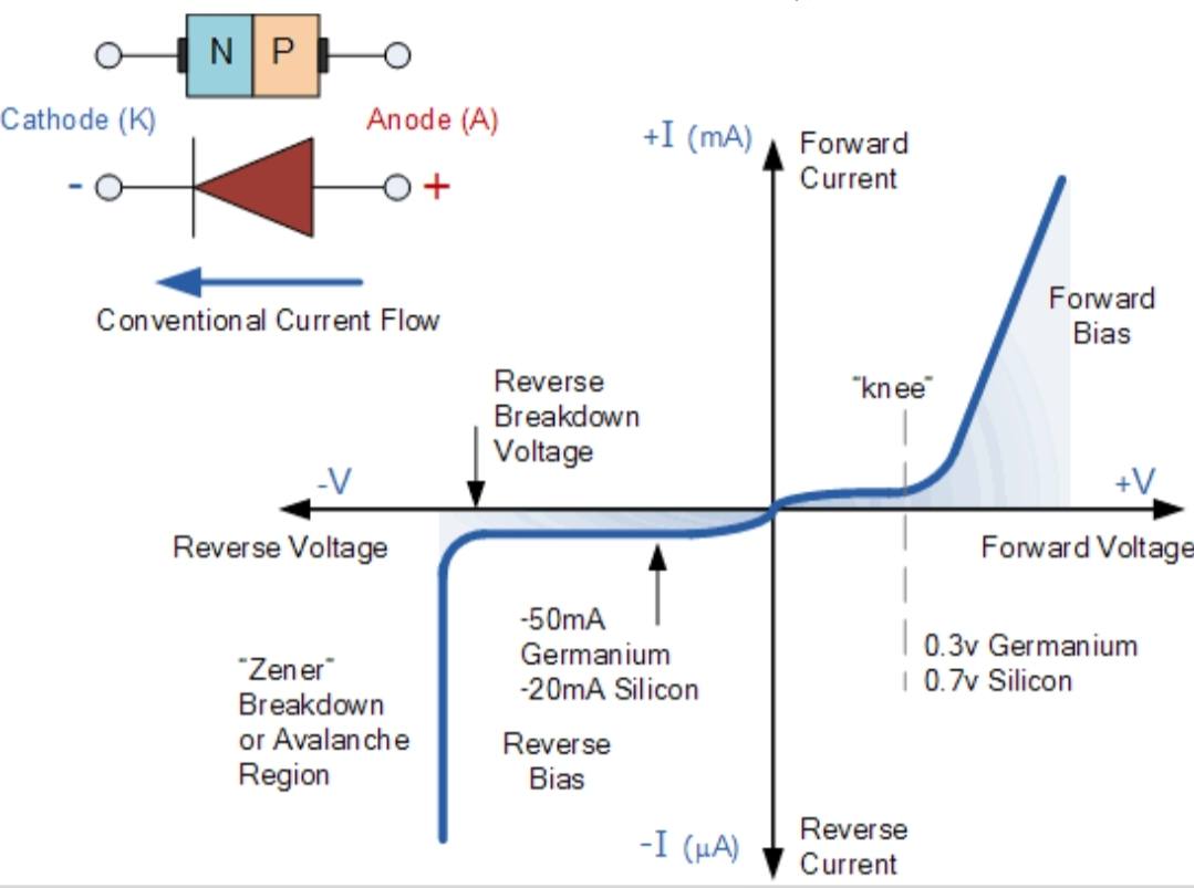
The behavior of a P-N junction Diode can be shown by V-I (voltage-current) characteristics:
The V-I characteristics can be divided into two parts
1.) Forward characteristics:
In forward direction as the voltage starts Increasing there are no changes in the current but as the voltage reaches V current starts increasing rapidly. Because there was a depletion region present between two materials, as the voltage increases the width of the depletion region decrease, at Voltage V (forward Voltage drop 0.7V for silicone and 0.3 for germanium), it vanishes completely and current starts increasing rapidly.

2.) Reverse characteristics:
In reverse direction as the voltage starts decreasing there is no current through the diode. However, there is a small current (from nano-ampers to micro-ampers due to minority carriers). If we keep on increasing the reverse voltage at very high voltage know as reverse-bias (nearly 140 volts for a silicon diode) Voltage the diode breaks and a very heavy current starts flowing through it.
Application of PN junction Diode
PN junction Diode is used in a vast variety of electronic and electrical circuits.
1.) Its major use is to block AC components in rectifiers used to convert AC to DC
2.) In demodulation of the carrier wave in receivers
3.) In frequency multiplier circuit
4.) LED are used as a light source
Working principle & Definition of diode
Hole-electron theory: watch this video
Definition of Diode, It’s a two-terminal polarized electronic component which mainly conducts current in one direction and blocks in other direction.
