When you are designing a printed circuit board (PCB), so much consideration is made on the placement of components, routing as well as the functionality but there are times that something has gone wrong and it is in the face of your eyes. Trace sizes, the length, width, and distance between the copper tracks on your circuit board can kill or make your design. A minor misplacement can plunge you into overheating, loss of signal or worse still, a terminal failure.
Have you ever asked yourself whether the reason that the culprit in your board behaves in a weird way may be the traces? Let’s dive in and unpack why getting these dimensions right really matters.
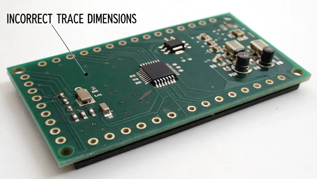
The Reason Trace Dimensions Are not mere Lines
One would want to imagine PCB traces to be nothing more than conductive lines moving electricity between points. They are actually highways that are very important in terms of signals and power. The width, thickness, and spacing are known to precisely define the current flow that is safe and the integrity of signals. If it is exceedingly small, traces heat up, and may be damaged. If it is excessively wide and you can have a hard time with constrained layouts or impedance differences.
These measurements are even more significant with different applications. High-frequency circuits, like RF circuits, are susceptible to cases of mismatch of impedance due to improper trace geometry. Power traces on any circuit board must have sufficient cross-sectional area to conduct current safely without voltage drop or overheating.
To the point, traces are not only the artwork of the board, but they determine performance and reliability directly.
Typical Issues of improper Dimensions
Trace dimension errors are the cause of mysterious failures that PCB designers have to deal with. These issues may be presented in different ways:
Overheating and Burnout: When a trace is too thin to carry the current it is carrying, resistance is greater, and heat is produced. This has the potential to wear out the board material in the long run or even burn the trace.
Signal Degradation: In high speed digital-to-analog signals, trace width and spacing affect impedance. Mismatched dimensions may result in reflections, distortion and loss of signal.
Electromagnetic Interference: Small traces can be a source of undesirable noise coupling between signals, especially in mixed-signal circuits.
Substandard performance in Power Delivery: Too-thin traces may cause voltage drops on sensitive components, causing instability.
These problems do not frequently manifest themselves immediately, so it is more difficult to diagnose them when no one thinks about the traces.
Trace Dimensions Determination
Trace dimensions cannot be determined by just guessing; it requires an electrical engineer with a calculator. The key factors include:
Existing Capacity Requirements: Depending on the anticipated load, the cross-sectional area of a trace should be able to support the current at a reasonable temperature increase.
Signal Speed and Frequency: High frequency signals demand-controlled impedance, that is dependent upon trace width, spacing, and dielectric thickness.
Manufacturing Constraints: PCB fabrication houses can support minimum width and minimum spacing, so your design selections are determined by this.
Environmental Conditions: The presence of harsh environments can necessitate thicker copper or broader traces to provide durability.
In case of power traces, calculated dimensions are frequently used, which depends on copper thickness and anticipated load, in formulas or a circuit board trace calculator. In the case of signal lines, a calculation of impedance may be required to adjust the system requirements.
The Trace Design Role of Impedance Matching
Impedance matching is not a radio engineering issue only, but also high-speed digital circuits are under very serious consideration. Trace impedance, as well as the dielectric of the board, is determined by the physical size of the trace. In the event of impedance mismatches, signals are not cleanly transmitted, but the signals reflect, giving rise to timing problems and corrupting data.
Specialized tools such as impedance matching tools can be used to compute and optimize your trace dimensions to achieve a particular signal integrity. This enables designers to adjust width and spacing prior to the commitment to fabrication, and this way gives high chances of being successful during the first pass.
Diagnosis of Suspected Trace Issues in a Board
What is the indicator of problematic trace dimensions? Here are some signs:
- Periodic load failures.
- Signals that appear healthy at low frequency but become poor at high frequency.
- Hotting out of local spots on the PCB.
- Shorted life of power parts without apparent reason.
When these indications indicate the physical layout, actual trace widths on the fabricated board can be compared against the design requirement, and differences can be found. Occasionally the manufacturing tolerances or variations in the etching work distort the desired dimensions. In some other instances, the initial design calculations were either wrong or optimistic.
Best Practices to prevent Dimension-Driven Failures
Early in the design, it is possible to prevent traces-related problems. Here is how you can keep ahead of the problem:
Before You Route: Use Design tools to Model thermal and electrical parameters before each critical trace is placed.
See Fabricator Guidelines: There is a minimum trace width, minimum spacing and minimum copper thickness limit in every PCB manufacturer.
Check with Calculators and Tools: It is always wise to check your dimensions with good buying calculators specific to handling or impedance control, or current.
Consider Accounting Tolerances of manufacture: Minimal variances during etching may affect high speed signals, therefore, remain within reasonable limits.
Test Prototypes Check, Check, Check: Before your products are even prototyped, check them against thermal cameras or signal integrity probes to make sure that your traces are acting in the manner you require.
Integrating these checks into your process significantly lowers the chance that such flaws go undetected to the point of making it to production.
Bringing It All Together
Are you getting faulty trace dimensions that are causing your board to fail? More designers are likely to think so. Subtle signal degradation, or even just burning out, can be the outcome of the incorrect width or spacing. Luckily nowadays, the tools and established design experiences allow these dimensions to be accurate at the first attempt.
The main point to note is that all traces form a part of your PCB circulatory system. Passionately treat them as precise as you are with component choice and schematic design. When your boards are acting oddly, be sure you consider the chances that the pathways themselves require some closer examination.
High Speed PCB Design: Essential Wiring Techniques for Optimal Performance
Gold Finger PCB Assembly: Best Practices for Ensuring Reliability
Revolutionary Axial Flux Printed Circuit Board (PCB) Stator Motor