This article explains an H-Bridge inverter circuit based on the SG3525 IC and MOSFETs like IRFZ44N or IRF3205 or IGBT like GT50JR22, which can convert DC to AC with a frequency of 50Hz or 60Hz, suitable for most standard applications. The SG3525 is a widely used PWM (Pulse Width Modulation) controller IC designed for various power electronics applications, including DC to AC inverters.
H-Bridge Inverter Circuit Overview
The SG3525-based H-Bridge inverter circuit converts low-voltage DC into high-voltage AC, making it ideal for use in applications like renewable energy systems, backup power supplies, and portable inverters. Below is a detailed description of the circuit components and their roles. You can also see block diagram of SPWM inverter circuit.
Components Required
- SG3525A PWM Controller IC
- N-channel MOSFETs (IRFZ44N or IGBT)
- Step-up Transformer (12V to 230V based on desired AC output voltage)
- Capacitors and Resistors (For filtering and frequency tuning)
- Diodes (1N4728A, 1N4733A Zener diodes and 1N4148 diode for protection)
- Inductors (Optional for output filtering)
- Power Supply (e.g., a 12V DC battery)
SG3525A IC Pinout Configuration
The SG3525 is a powerful PWM controller IC designed for efficient energy conversion. It offers features like an internal oscillator, soft start, under-voltage lockout, and shutdown capabilities. Here’s an overview of its pin functions:
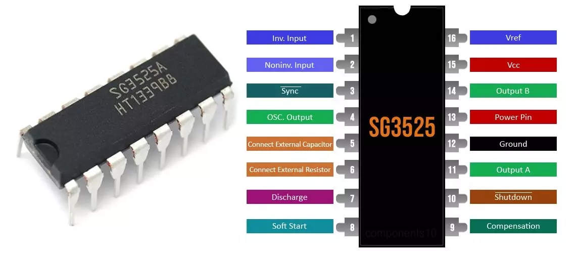
- Pin 1 (INV): Inverting input of the error amplifier, typically connected to the feedback signal.
- Pin 2 (NI): Non-inverting input of the error amplifier, often tied to a reference voltage.
- Pin 3 (SYNC): Synchronization pin for external clock inputs.
- Pin 4 (OSC): Pin for connecting the timing capacitor, used to set the oscillator frequency.
- Pin 5 (CT): Timing capacitor pin for controlling the internal oscillator frequency.
- Pin 6 (RT): Timing resistor pin for oscillator frequency adjustment.
- Pin 7 (DISCHARGE): Discharges the timing capacitor during each oscillator cycle.
- Pin 8 (SOFT-START): Controls the startup process with a capacitor to ensure a gradual increase in output.
- Pin 9 (COMP): For feedback loop stability and compensation.
- Pin 10 (SHUTDOWN): Activates the shutdown feature to disable the output stages immediately.
- Pins 11 & 14 (OUT A, OUT B): PWM outputs to drive external MOSFETs.
- Pin 12 (VCC): Main supply voltage input.
- Pin 13 (GND): Ground connection.
- Pin 15 (VC): Supply voltage for the output stage.
- Pin 16 (VREF): Provides a 5V reference for external components.
Setting the PWM Frequency
The PWM frequency of the SG3525 is determined by external timing components resistors and capacitor (RT and CT) connected to Pins 5 and 6. The following formula calculates the oscillator frequency:
F = 1 / (CT × (0.7 RT + 3 RD))
Where:
- F = Frequency in Hz
- CT = Timing Capacitor (F)
- RT = Timing Resistor (Ω)
- RD = Deadtime Resistor between pins 5 & 7 (Ω)
For example, with the following component values:
- CT = 1µF
- RT = 14kΩ
- RD = 47Ω
Substituting these into the formula:
F = 1 / (1 × 10⁻⁶ × (0.7 × 14 × 10³ + 3 × 47))
F ≈ 100.59Hz
This frequency can be adjusted depending on the application requirements, such as 50Hz or 60Hz for AC power output.
Designing The H-Bridge Inverter Circuit Using IC SG3525
The SG3525 IC when combined with an H-bridge configuration of complementary MOSFETs, becomes an efficient solution for converting DC voltage to AC power. With the integration of additional components for output voltage regulation and low battery cut-off, the circuit can ensure reliable performance and protection for connected devices.
Key Components of H-Bridge Inverter Circuit
The H-bridge inverter circuit comprises several critical components, each contributing to the efficient operation of the system. Below is an overview of the primary elements:
- SG3525 IC: The main controller for generating PWM signals to drive the MOSFETs in the H-bridge configuration.
- H-Bridge MOSFETs: Power transistors (typically N-channel MOSFETs such as IRFZ44N or IRF3205) that switch the DC voltage to generate an alternating waveform.
- Driver Circuit: Interfaces the SG3525 with the MOSFETs to ensure proper switching.
- Step-Up Transformer: Converts the low-voltage DC input into higher-voltage AC output.
- Voltage Feedback Circuit: Ensures output voltage regulation by adjusting the PWM duty cycle.
- Low Battery Cut-Off Circuit: Disconnects the load when the battery voltage falls below a safe threshold, protecting the battery from over-discharge.
- Protection Circuits: Provides safeguards against overcurrent, overheating, and short circuits (optional).
- Low-Pass Filter: Converts the PWM signal into a smoother AC waveform for sensitive devices (optional).
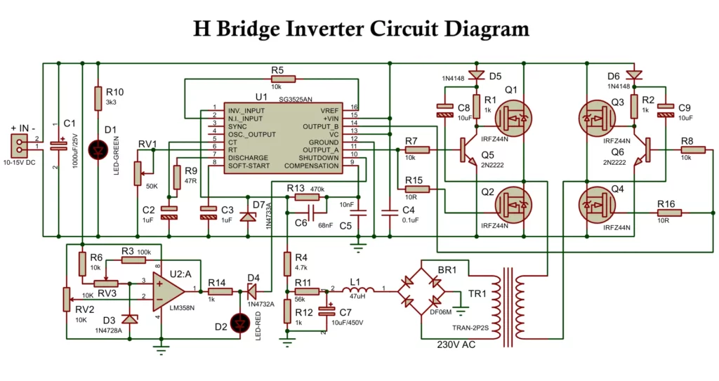
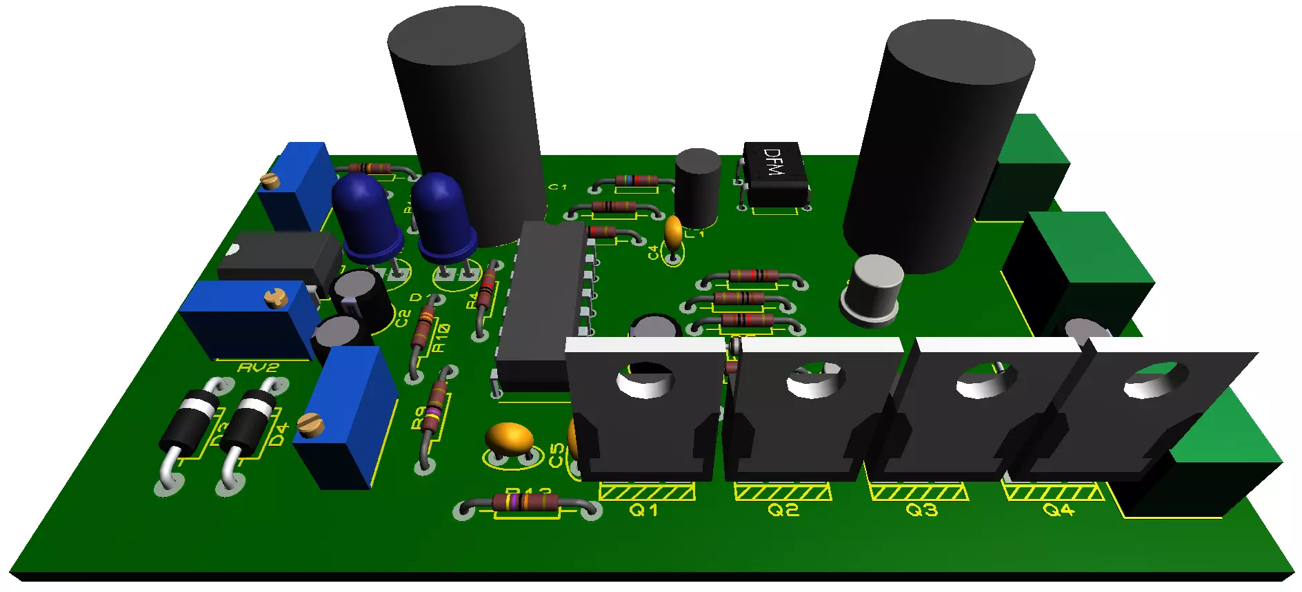
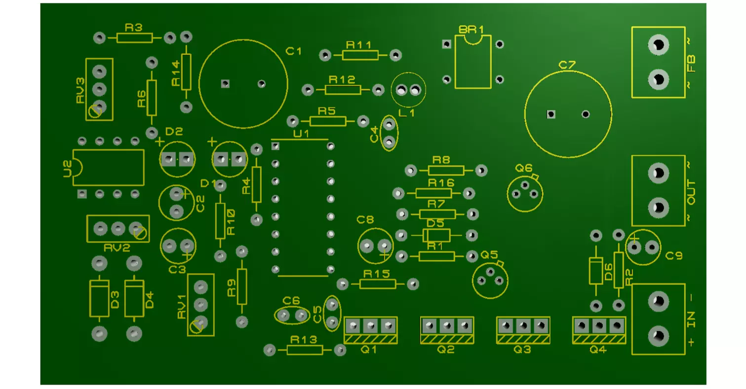
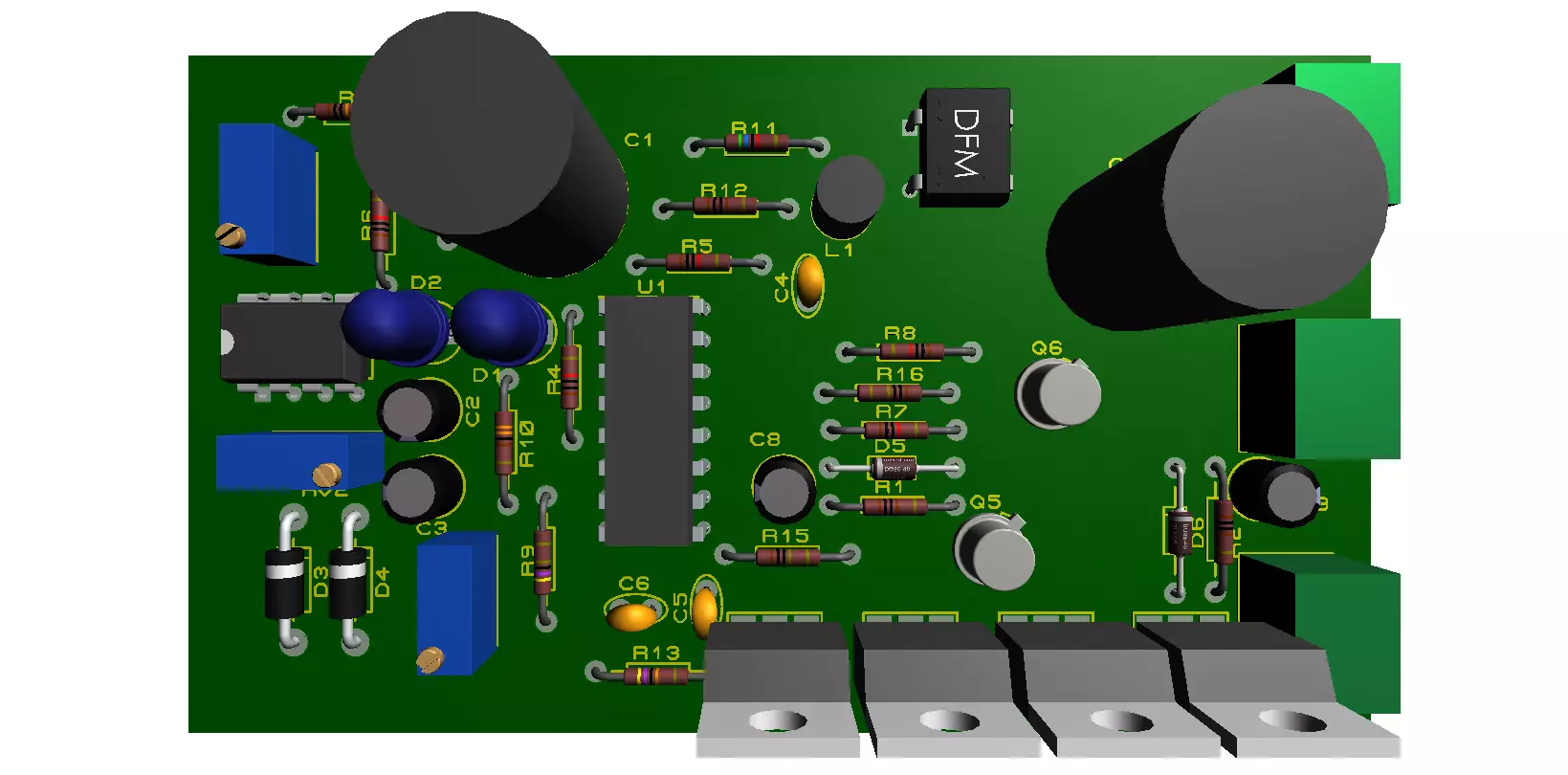
SG3525 Based H Bridge Inverter Circuit Schematic
Below is the schematic description of the SG3525 based H-bridge inverter circuit:
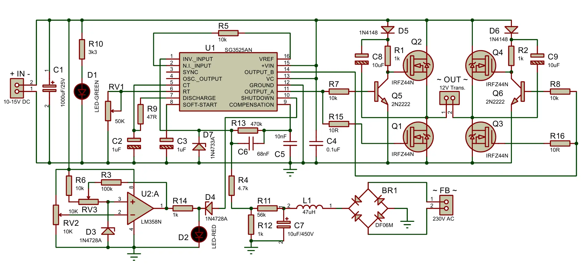
Component List
- Resistors:
- R1, R2 = 1kΩ
- R3 = 100kΩ
- R4 = 4.7kΩ(current limiting, not fixed)
- R5, R6, R7, R8 = 10kΩ
- R9 = 47Ω
- R10 = 3.3kΩ
- R11 = 56kΩ
- R12, R14 = 1kΩ
- R13 = 470kΩ
- R15, R16 = 10Ω
- RV1 = 50kΩ preset
- RV2, RV3 = 10kΩ presets
- Capacitors:
- C1 = 1000µF/25V
- C2, C3 = 1µF
- C4 = 0.1µF
- C5 = 10nF
- C6 = 68nF
- C7 = 10µF/450V
- C8, C9 = 10uF
- Inductor: L1 = 47µH
- Diodes:
- D1 = Green LED
- D2 = Red LED
- D3, D4 = 1N4728A Zener
- D5, D6 = 1N4148
- D7 = 1N4733A
- Transistors and ICs:
- Q1, Q2, Q3, Q4 = IRFZ44N MOSFETs
- Q5, Q6 = 2N2222
- U1 = SG3525A IC
- U2 = LM358 or LM393
- Other Components:
- 12V to 220V step up transformer
- 12V battery
- Screw terminals (2, 2, 2)
Detailed Working of SG3525 H Bridge Inverter Circuit
1. SG3525 PWM Controller
The SG3525 IC serves as the core of the circuit, generating complementary PWM signals for driving the MOSFETs in the H-bridge configuration.
- Pin 1 (INV) and Pin 2 (NI): These inputs are used for feedback control to regulate the output voltage. A voltage divider circuit from the output provides a feedback signal to the error amplifier, which adjusts the PWM duty cycle.
- Pin 5 (Oscillator Timing Capacitor): A capacitor connected here determines the oscillator frequency, typically set for a 50 Hz AC output.
- Pin 6 (Oscillator Timing Resistor): Works with the timing capacitor to set the frequency.
- Pin 8 (Soft Start): A capacitor connected to this pin controls the gradual ramp-up of PWM signals, reducing the risk of inrush current.
- Pin 9 (COMP): This pin allows loop stability through compensation.
- Pin 10 (Shutdown): Used for disabling the PWM outputs when the low battery cut-off is activated.
- Pins 11 and 14 (Outputs A & B): Provide complementary PWM signals to drive the gates of the MOSFETs.
2. H-Bridge MOSFET Power Stage
The H-bridge stage consists of four N-channel MOSFETs (e.g., IRFZ44N), which switch the DC voltage across the transformer’s primary winding to generate an alternating waveform.
- Gate Resistors: Resistors are connected to the MOSFET gates to limit the gate charging current and prevent ringing.
- Flyback Diodes: Diodes across the MOSFETs protect them from voltage spikes caused by the inductive nature of the transformer.
3. Step-Up Transformer
A 12V to 230V step-up transformer is used to convert the low-voltage DC input (typically 12V to 15V) into high-voltage AC output (220V to 240V). The turns ratio of the transformer must match the desired output voltage.
- The MOSFETs drive the transformer’s primary winding, and the secondary winding delivers the required AC output.
- Connect the 12V battery to the input terminal and the transformer’s primary terminals to the H-bridge’s output terminals.
4. Output Voltage Regulation
Voltage regulation is achieved using a feedback circuit. A voltage divider network on the transformer’s secondary (AC output) reduces the output voltage to a suitable level for the SG3525’s feedback input. This feedback signal is fed to the error amplifier (Pin 1), allowing the IC to adjust the PWM duty cycle and maintain a stable output voltage.
5. Low Battery Cut-Off Circuit
A low battery cut-off circuit protects the battery from over-discharge.
- Voltage Divider for Monitoring: A resistor divider reduces the battery voltage for comparison.
- Comparator Circuit: An operational amplifier (e.g., LM358 or LM393) monitors the battery voltage. When the voltage drops below a preset threshold (e.g., 10.5V for a 12V battery), the comparator pulls the SG3525’s shutdown pin (Pin 10) high, disabling the PWM outputs.
- Zener Diode: 1N4728A diode provides a stable reference voltage for comparison and protects the IC.
6. Optional Features
- Low-Pass Filter: To smooth the PWM waveform into a sinusoidal shape, an LC filter (inductor and capacitor) can be added to the circuit. This is particularly useful for sensitive devices requiring pure sine wave output.
- Protection Circuits: Overcurrent protection and short-circuit protection can be added to safeguard the MOSFETs and other components.
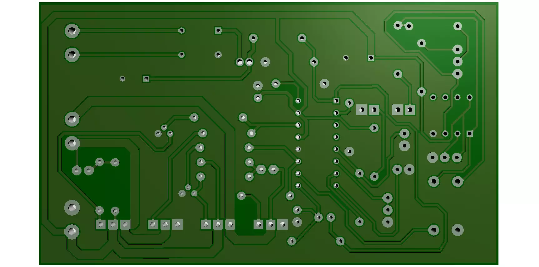
PCB Design and Assembly
PCB Layout
The inverter circuit can be implemented on a PCB with thick copper traces to handle high current. Soldering the tracks can further enhance current-carrying capacity.
Connections
- Connect the transformer output to the feedback input terminal.
- Ensure proper heat dissipation for the MOSFETs by attaching heatsinks to manage thermal performance.
Considerations for Reliable Operation
- Feedback Accuracy: Ensure precise feedback for stable voltage regulation and consistent output frequency.
- Thermal Management: Use adequate heatsinks for the MOSFETs to prevent overheating during operation.
- Component Ratings: Select components with appropriate voltage and current ratings to match the load requirements.
- Testing: Before connecting a load, test the circuit thoroughly to ensure proper operation and safety.
Conclusion
The SG3525-based H-bridge inverter circuit is a reliable and efficient solution for converting DC voltage to AC power. With features such as voltage regulation and low battery protection, it is suitable for powering a wide range of devices. By incorporating additional modifications, such as an SPWM generator or low-pass filters, the circuit can produce pure sine wave outputs, making it ideal for sensitive appliances. This circuit is an excellent choice for various inverter applications, from basic setups to advanced systems requiring enhanced functionality and safety features.