Wireless projects are always fascinating, adding flexibility and convenience to electronics applications. Among various wireless technologies, RF modules are widely used due to their simplicity and affordability. In this project, we will build a 433MHz RF transmitter and receiver circuit to control LEDs wirelessly. This guide will cover the components required, circuit design, and working principle of RF communication.
433MHz RF Transmitter and Receiver Circuit
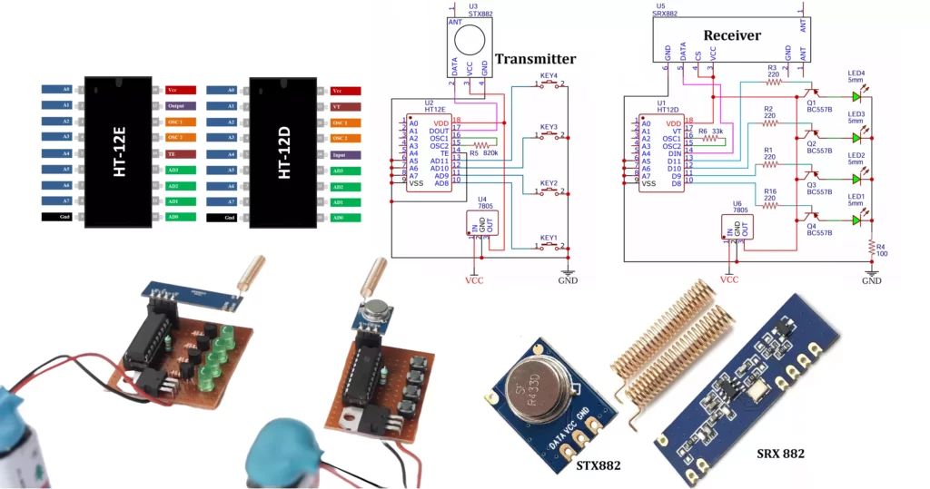
A 4-Channel RF Transmitter and Receiver Circuit enables wireless control over four separate devices, utilizing components like the 433 MHz RF module, HT12E encoder, and HT12D decoder ICs. This configuration is widely applied in areas such as home automation, robotics, and security systems.
Components and Their Functions
- 433 MHz RF Transmitter STX882 and Receiver SRX882 Modules: Facilitate wireless communication between the transmitter and receiver units.
- HT12E Encoder IC: Encodes 4-bit parallel data into serial form for transmission.
- HT12D Decoder IC: Decodes the received serial data back into 4-bit parallel form.
- 18-pin IC Bases (x2): Provide a removable interface for the ICs.
- Momentary Push Buttons (x4): Serve as input controls for the transmitter.
- LEDs (x5): Indicate the status of each channel and valid transmission.
- Resistors: 1 MΩ for the HT12E oscillator, 33 KΩ for the HT12D oscillator, and 470 Ω for current limiting with LEDs.
- IC 7805 Voltage Regulators (x2): Regulate the 9V battery input to a stable 5V supply.
- 9V Batteries (x2): Provide power to the transmitter and receiver circuits.
- Battery Connectors (x2): Connect the batteries to the circuits.
- Breadboard or Vero Board: For assembling the circuit.
- Connecting Wires: Establish electrical connections between components.
HT12E & HT12D ICs Pinout Description
The HT12E (Encoder) and HT12D (Decoder) commonly facilitate wireless data transmission in RF communication applications, particularly in 433MHz and 315MHz RF modules. These ICs encode and decode 12-bit data, but only 4 bits are for actual data transmission remaining 8 bits are address.
HT12E (Encoder) Pinout & Description
The HT12E encoder converts parallel data from input switches or sensors into a serial data stream that is transmitted wirelessly via an RF module.
| Pin No. | Pin Name | Description |
|---|---|---|
| 1-8 | A0 – A7 | Address Pins: Used for security purposes; should match with the HT12D decoder. Can be connected to VCC or GND. |
| 9 | Ground (VSS) | Ground pin (0V). |
| 10-13 | Data Input (D0 – D3) | Data Pins: These inputs are used to send data (ON/OFF from switches, sensors, etc.). |
| 14 | Transmission Enable (TE) | Active low. When pulled low, the encoder transmits the data. |
| 15 | Oscillator Output (OSC2) | External resistor (typically 1MΩ) is connected here to set the internal oscillator frequency. |
| 16 | Oscillator Input (OSC1) | External resistor is connected oscillator pin. |
| 17 | Data Output (DOUT) | Outputs the encoded serial data, which is transmitted by an RF module. |
| 18 | VCC | Power supply (3V-12V DC). |
HT12E Typical Connection Diagram
- Address pins (A0-A7): Must be the same for both encoder and decoder.
- Data pins (AD8-AD11): Connected to switches or microcontroller outputs.
- TE pin: Pulled low to enable transmission.
- DOUT: Connected to the RF transmitter module.
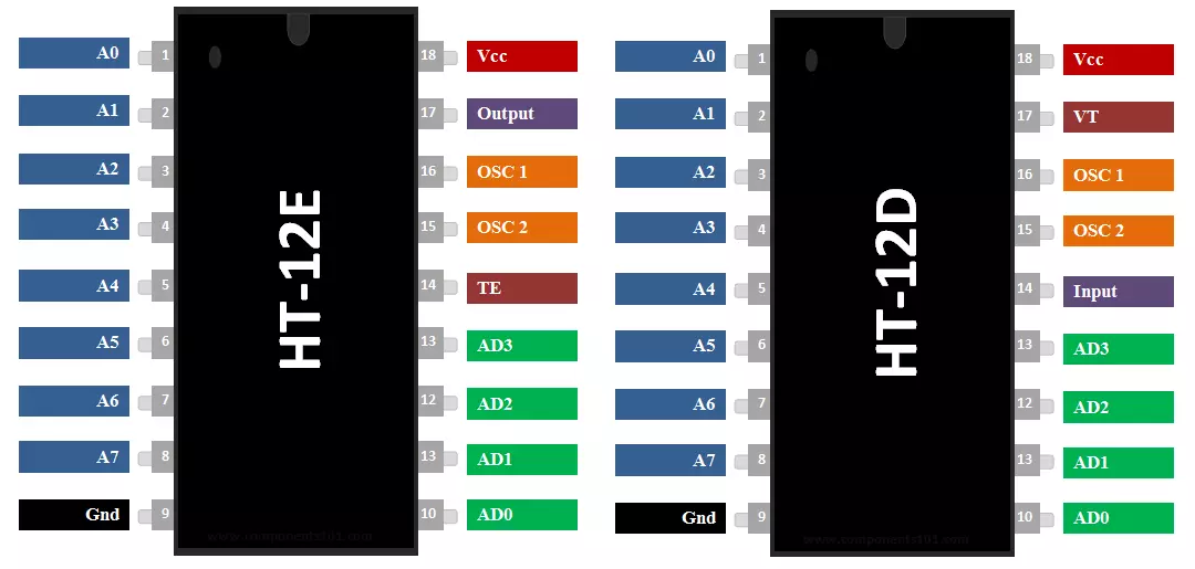
HT12D (Decoder) Pinout & Description
The HT12D decoder receives the serial data from an RF module, decodes it, and provides the parallel output.
| Pin No. | Pin Name | Description |
|---|---|---|
| 1-8 | A0 – A7 | Address Pins: Should match the encoder (HT12E). |
| 9 | Ground (VSS) | Ground pin (0V). |
| 10-13 | Data Output (D0 – D3) | Outputs the received data in parallel form (for motor control, LEDs, etc.). |
| 14 | Serial Data Input (DIN) | Receives the encoded serial data from an RF receiver module. |
| 15 | Oscillator Output (OSC2) | External resistor (typically 51KΩ) is connected here to set the internal oscillator frequency. |
| 16 | Oscillator Input (OSC1) | External resistor is connected oscillator pin. |
| 17 | Valid Transmission (VT) | Active high when a valid signal is received. Can be used to trigger an indicator (LED/buzzer). |
| 18 | VCC | Power supply (3V-12V DC). |
HT12D Typical Connection Diagram
- DIN: Connected to the RF receiver module.
- VT (Valid Transmission): Goes HIGH when valid data is received.
- Data Outputs (D0-D3): Drive relays, LEDs, or other control circuits.
Working of HT12E and HT12D
- HT12E (Encoder)
- Takes 4-bit parallel data and an 8-bit address.
- Encodes and transmits serial data via the RF module when TE is low.
- HT12D (Decoder)
- Receives serial data from the RF receiver.
- If the received address matches its own, it decodes the data and sets VT high.
- Outputs the decoded data on D0-D3.
HT12E & HT12D Applications
Wireless remote-control systems
RF-based home automation
Remote switching applications
Car security systems
Wireless alarm systems
433MHz RF Transmitter & Receiver Modules
The 433MHz RF Transmitter & Receiver modules play a crucial role in wireless communication for home automation, remote control systems, and other low-power applications. These modules work in ASK (Amplitude Shift Keying) / OOK (On-Off Keying) modulation.
433MHz RF Transmitter Module (STX882)
The 433MHz Transmitter module is responsible for sending data wirelessly. It operates at 3V – 12V and transmits data using ASK modulation.
Pinout and Description
| Pin No. | Pin Name | Description |
|---|---|---|
| 1 | Antenna (ANT) | Connect a 17.3 cm wire or an external antenna for better range. |
| 2 | Data (DIN) | Input pin for data from HT12E encoder or microcontroller (e.g., Arduino, PIC). |
| 3 | VCC | Power supply (3V – 12V DC) (Higher voltage = Longer range). |
| 4 | Ground (GND) | Ground connection (0V). |
Features
Transmission Range: Up to 100 meters (with a proper antenna).
Frequency: 433MHz
Power Consumption: Low power operation
Modulation: ASK / OOK
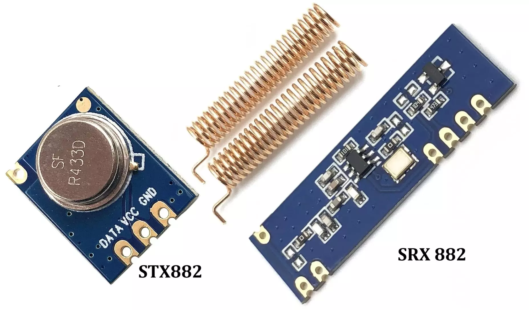
433MHz RF Receiver Module (SRX882)
The 433MHz Receiver module receives the transmitted data and outputs it for further processing.
Pinout and Description
3VCCPower supply (5V DC) (Do not exceed 5V).
| Pin No. | Pin Name | Description |
|---|---|---|
| 1 | Antenna (ANT) | Connect a 17.3 cm wire or an external antenna for better reception. |
| 2, 6 | GND | Ground connection (0V). |
| 4 | CS | Chip select 1: normal working 0: sleep |
| 5 | Data (DOUT) | Output pin for decoded data. |
Features
Operating Voltage: 5V DC
Reception Range: Up to 100m (with an antenna)
Sensitivity: -105 dBm
Modulation: ASK / OOK
Multiple Data Outputs: Can be connected to HT12D decoder or microcontroller.
Working
- HT12E (Encoder) + 433MHz Transmitter
- The HT12E takes 4-bit parallel data and encodes it into a serial signal.
- The 433MHz Transmitter sends this serial data wirelessly.
- 433MHz Receiver + HT12D (Decoder)
- The 433MHz Receiver gets the serial data.
- The HT12D decodes it and converts it back to 4-bit parallel data.
RF Transmitter and Receiver Circuit Explanation
Transmitter Section
- Power Supply: A 9V battery supplies power, regulated to 5V by the IC 7805 to ensure consistent voltage for the circuit components.
- HT12E Encoder IC: This IC encodes the 4-bit parallel input from the push buttons into a serial data stream suitable for RF transmission.
- Push Buttons: Each button corresponds to one of the four channels. Pressing a button sends a LOW signal to the HT12E, initiating data transmission.
- 433 MHz RF Transmitter Module: Transmits the encoded serial data wirelessly to the receiver module.
- Address Pins (A0–A7): These pins set the address for communication. Both the encoder and decoder must share the same address configuration to ensure proper pairing.
- Oscillator Resistor: A 1 MΩ resistor connected to the oscillator pin of the HT12E sets the internal clock frequency, crucial for timing the data transmission.
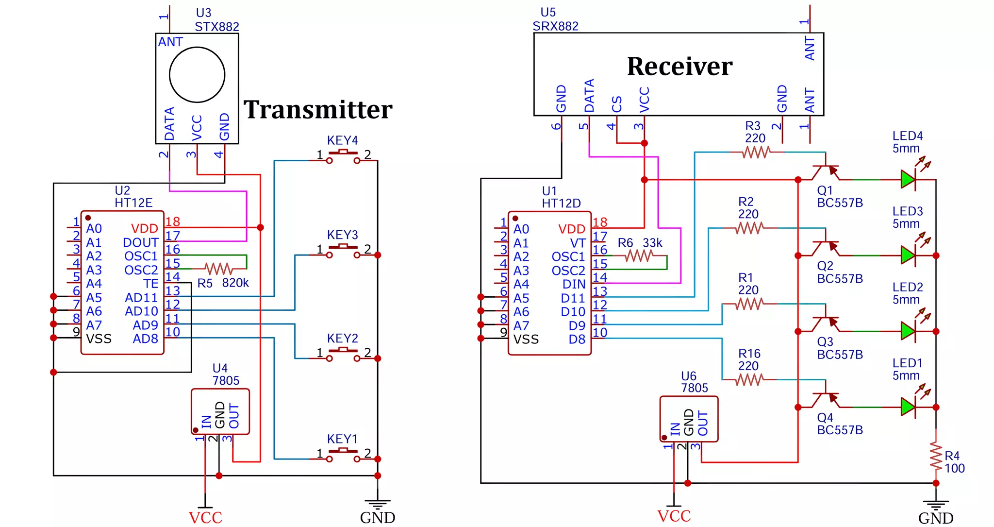
Receiver Section
- Power Supply: Similar to the transmitter, a 9V battery regulated to 5V by an IC 7805 powers the receiver circuit.
- 433 MHz RF Receiver Module: Captures the transmitted RF signals and forwards the serial data to the HT12D decoder IC.
- HT12D Decoder IC: Decodes the received serial data back into 4-bit parallel form, corresponding to the original input from the transmitter’s push buttons.
- LED Indicators: Each of the four LEDs connects to an output pin of the HT12D, lighting up to indicate activation of the corresponding channel.
- Oscillator Resistor: A 33 KΩ resistor connected to the oscillator pin of the HT12D sets its internal clock frequency, ensuring proper data decoding.
- Valid Transmission (VT) Indicator: An additional LED connected to the VT pin of the HT12D lights up when it receives valid data, confirming successful communication.
Working of RF Transmitter and Receiver Circuit
- Initiating Transmission: Pressing a push button on the transmitter sends a LOW signal to the corresponding data pin on the HT12E encoder.
- Encoding: The HT12E encodes this input into a serial data stream, including the address and data bits, and sends it to the RF transmitter module.
- Wireless Transmission: The 433 MHz RF transmitter module broadcasts the encoded signal wirelessly.
- Reception: The RF receiver module captures the transmitted signal and passes it to the HT12D decoder.
- Decoding: The HT12D decodes the serial data back into parallel form. If the address bits match its configured address, it considers the data valid.
- Output Activation: The HT12D activates the corresponding output pin, lighting up the associated LED to indicate the received command.
- Valid Transmission Indication: The VT pin goes HIGH, lighting the VT indicator LED to confirm successful data reception.
Address Configuration
Both HT12E and HT12D must have the same address settings (A0-A7) for proper communication. These address pins are typically grounded (00000000).
Testing and Implementation
Initially, the circuit is tested on a breadboard before designing it on a veroboard for a permanent setup. Adding a 17cm antenna increases the working range up to 50 meters.

Advantages of RF Transmitter and Receiver Circuit
- Wireless Operation: Eliminates the need for physical wiring between control and device, offering flexibility in device placement.
- Multiple Device Control: Capable of controlling up to four devices independently, enhancing versatility.
- Cost-Effective Components: Utilizes affordable and readily available components, making it accessible for hobbyists and professionals alike.
- Low Power Consumption: Efficient design suitable for battery-powered applications, extending operational life.
- Simplicity in Design: Straightforward circuit design allows for easy assembly and troubleshooting.
Disadvantages of RF Transmitter and Receiver Circuit
- Potential Interference: RF signals are susceptible to interference from other electronic devices and physical obstructions, which can affect performance.
- Security Concerns: Hackers can intercept signals without proper encoding, creating security risks in sensitive applications.
- Limited Range: Obstacles and interference can reduce the circuit’s effective range.
Applications of RF Transmitter and Receiver Circuit
- Remote control (Toys, Garage doors, Fans, Lights)
- Wireless security systems
- Home Automation
- Doorbells
- Short-range data transmission
- Remote control of household appliances
- Smart IoT applications
Conclusion
Building a 433MHz RF transmitter and receiver circuit is an excellent way to explore wireless communication. With a simple design and affordable components, this circuit offers a reliable solution for remote control applications. By following the steps outlined, you can successfully construct and test the system for various wireless projects. Whether for hobbyist experiments or practical applications, this RF circuit provides a solid foundation for learning and innovation.
FAQs on RF Transmitter and Receiver Circuit
How much is the cost of this circuit?
This Circuit will cost you around 5$ to 7$.
What is the range of this circuit?
The working range is up to 100 meters with a proper antenna setup.
Can I use this circuit to control AC appliances?
Yes! You can replace the LEDs with relays to control AC appliances wirelessly. This project is an excellent introduction to RF communication and can be extended for various IoT and automation applications.
If you have any doubts, feel free to ask in the comments. Happy building!
Interfacing DHT11 + Soil Moisture Sensor with Arduino & ESP32