Let’s see SR latch and explore SR flip flop truth table, with its working, advantages, limitations and applications. The SR flip-flop, also known as the Set-Reset flip-flop, is a fundamental building block in digital electronics used for storing a single bit of data. This type of flip-flop has two inputs labeled S (Set) and R (Reset), along with two outputs: Q and Q’ (the complement of Q). It’s widely used in memory storage devices, registers, and sequential circuits.
Logic Symbol and Truth Table of SR Latch/Flip-Flop:
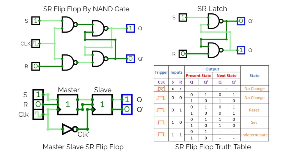
The truth table and logic symbol for an SR flip-flop is shown below:

Components:
- S (Set) Input: Used to set the output Q to 1.
- R (Reset) Input: Used to reset the output Q to 0.
- Q (Output): Stores the data (either 1 or 0).
- Q’ (Complement of Output): Always the opposite of Q.

Explanation:
- S = 0, R = 0 (Hold State): When both S and R are 0, the latch remains in its previous state. It holds its current value.
- S = 0, R = 1 (Reset State): The latch is reset, meaning the output Q is forced to 0, and Q’ becomes 1.
- S = 1, R = 0 (Set State): The latch is set, which means the output Q is set to 1, and Q’ becomes 0.
- S = 1, R = 1 (Invalid State): Both S and R being 1 results in an invalid state where both Q and Q’ are undefined. In practical circuits, this condition is avoided because it leads to unpredictable behavior.
Circuit Diagram of SR Flip-Flop:
The SR flip-flop can be implemented using either NAND gates or NOR gates. Let’s explore both implementations:
1. SR Flip-Flop using NAND Gates:
In this configuration, the SR flip-flop consists of two cross-coupled NAND gates. Here, the inputs are active-low, meaning a 0 activates the input.

2. SR Flip-Flop using NOR Gates:
This implementation uses two cross-coupled NOR gates, with active-high inputs.

Working of NOR Gate SR Flip-Flop:
1. Initial State
- When power is first applied to the circuit, the state of Q and Q’ depends on the input condition at the S and R terminals.
- If S and R are both low (0), the output holds the previous state.
2. Set State (S = 1, R = 0)
- The Set input (S) triggers the flip-flop to output a 1 on Q and a 0 on Q’. This is known as the “Set” state, meaning the flip-flop is storing a logic 1.
3. Reset State (S = 0, R = 1)
- When R is high (1) and S is low (0), the flip-flop enters the “Reset” state, meaning Q is set to 0 and Q’ to 1.
4. Hold State (S = 0, R = 0)
- In the hold state, both inputs are low (0), and the flip-flop retains its previous state. The output does not change in this condition, making it a memory element.
5. Invalid State (S = 1, R = 1)
- When both Set and Reset are 1, the outputs Q and Q’ become undefined, leading to an invalid or forbidden state. In practical designs, this condition is avoided using additional logic or constraints.
SR Flip Flop Truth Table:

SR Flip-Flop Excitation Table:
The excitation table of an SR flip-flop defines the required inputs (S and R) to transition the flip-flop from its current state (Qn) to a desired next state (Qn+1). This table is crucial in designing sequential circuits because it tells us what input values are needed to achieve a specific output change.
| Qn | Qn+1 | S | R |
|---|---|---|---|
| 0 | 0 | 0 | 0 |
| 0 | 1 | 1 | 0 |
| 1 | 0 | 0 | 1 |
| 1 | 1 | 0 | 0 |
Explanation of Each Row
- Hold State (No Change): When Qn = 0 and Qn+1 = 0, S and R both need to be 0 to maintain the current state. Similarly, when Qn = 1 and Qn+1 = 1, both S and R should also be 0 to hold the state.
- Set State: To change from Qn = 0 to Qn+1 = 1, we need to set S = 1 and R = 0.
- Reset State: To change from Qn = 1 to Qn+1 = 0, we need to set S = 0 and R = 1.
This excitation table is instrumental in circuit design and helps determine the required input values for achieving specific output states in sequential logic applications.
Master-Slave SR Flip-Flop:
The Master-Slave SR flip-flop is a configuration that addresses timing issues in traditional SR flip-flops, enabling them to work synchronously with clock signals. This setup consists of two SR flip-flops connected in series: the Master and the Slave.
Structure of Master-Slave SR Flip-Flop:
In a Master-Slave SR flip-flop:
- Master flip-flop: It captures the inputs S and R during the positive (rising) edge or high phase of the clock.
- Slave flip-flop: It changes its output based on the master’s output during the negative (falling) edge or low phase of the clock.
This configuration allows the flip-flop to change its output only once per clock cycle, avoiding potential timing issues.

Working of Master-Slave SR Flip-Flop:
The Master-Slave SR flip-flop works in two phases of a clock cycle:
Clock High (Master Active):
- During the high phase of the clock, the Master flip-flop is active and responds to the inputs S and R.
- The Slave flip-flop is inactive and does not change its output at this time.
- The Master flip-flop captures the current input state but does not immediately transfer it to the output.
Clock Low (Slave Active):
- During the low phase of the clock, the Slave flip-flop becomes active and takes the output state of the Master flip-flop.
- This delayed transfer ensures that the output Q and Q’ only update based on the captured inputs from the previous clock high phase.
- This two-stage process prevents any glitches in the output caused by brief input changes during the clock cycle.
Master-Slave SR Flip Flop Truth Table:
The truth table of a Master-Slave SR flip-flop is similar to a basic SR flip-flop with an additional clock input. The output changes only during the low phase of the clock.
| Clock | S | R | Master State | Slave State | Output Q | Description |
|---|---|---|---|---|---|---|
| High | 0 | 0 | Hold | No Change | Hold | Hold Previous State |
| High | 0 | 1 | Reset | No Change | Reset | Reset Q = 0 |
| High | 1 | 0 | Set | No Change | Set | Set Q = 1 |
| High | 1 | 1 | Invalid | No Change | Invalid | Not Allowed |
| Low | X | X | Hold | Follows Master | Updated | Updates Output |
- High Clock Phase: The master flip-flop responds to inputs S and R to capture the state, but the output does not update immediately.
- Low Clock Phase: The slave flip-flop copies the state from the master flip-flop, and the output Q changes.
Need for Master-Slave Configuration:
The Master-Slave configuration solves a few key problems with the basic SR flip-flop:
Timing Issues:
- In a simple SR flip-flop, the output may respond immediately to changes in inputs, which can lead to race conditions or unintended changes.
- The Master-Slave arrangement ensures output changes only once per clock cycle, improving synchronization.
Glitch Prevention:
- Input signals often have glitches or temporary fluctuations, which can cause the output to toggle unexpectedly in a simple SR flip-flop.
- With the Master-Slave configuration, only the input state at the clock edge is captured, preventing glitches from affecting the output.
Controlled State Change:
- In sequential circuits, it’s essential to control when the flip-flop updates to maintain a reliable circuit.
- Master-Slave flip-flops ensure that outputs are only updated at a predictable time, making them ideal for synchronous digital circuits.
ICs Which can be used as SR Latch or Flip Flop:
- TTL Logic (7400 series): IC 7400, IC 7402, IC 74279
- CMOS Logic (4000 series): CD4043, CD4044, CD4001
- Adaptable Flip-Flop ICs: IC 555 Timer, IC 7473, IC 7474
These flip flop ICs are used in digital circuits for storage, logic processing, and control applications.
Advantages of SR Flip-Flop:
- Simple Design: Easy to understand and build, usually requires only two NAND or NOR gates.
- Basic Memory Storage: Can store a single bit (0 or 1), useful for building larger memory systems.
- Foundation for Other Flip-Flops: The SR flip-flop is the base for more advanced types like JK, D, and T flip-flops.
- Useful in Simple Latch Circuits: Ideal for basic circuits needing a simple “on/off” latch, like switch debouncing.
Disadvantages of SR Flip-Flop:
- Undefined State: When both Set (S) and Reset (R) are active, the output becomes unpredictable.
- Limited Application: SR flip-flops are not ideal for complex circuits; JK or D flip-flops work better in those cases.
- No Clock Control: Works based on input levels, not on clock signals, which can cause timing issues.
- Sensitive to Noise: Noise on S and R inputs can cause accidental changes in state.
- Extra Circuitry for Clocking: Needs additional circuitry to work well with clocked or synchronized systems.
In short, SR flip-flops are simple but limited, making them useful in basic applications but unsuitable for complex, timing-sensitive systems.
Applications of SR Flip-Flop:
SR flip-flops (Set-Reset flip-flops) are basic memory elements used widely in digital electronics for storing and controlling binary data. Here are some of their key applications:
1. Data Storage
- SR flip-flops store a single bit of data (1 or 0) and can maintain their state until they are reset or set again.
- Used in simple storage circuits and in registers as a building block for more complex data storage solutions.
2. Latch and Memory Elements
- SR flip-flops are often used in latching applications, where the goal is to maintain a certain state until a control signal changes it.
- They are ideal for temporary storage of data, especially in memory cells within registers or buffers in microcontrollers.
3. Basic Building Blocks for More Complex Flip-Flops
- The SR flip-flop is a foundational flip-flop from which other types, like D, JK, and T flip-flops, are derived.
- This makes them crucial in the design and understanding of more complex flip-flop circuits.
4. Debouncing Mechanical Switches
- SR flip-flops are often used in debouncing circuits to stabilize the input from mechanical switches.
- A mechanical switch may create multiple ON/OFF signals (bounce) when pressed, and an SR flip-flop can help ignore these unwanted changes, providing a clean output.
5. Control Circuits for Power and System Reset
- They are used in control circuits to create stable outputs that only change with specific conditions, ideal for system initialization and power-on reset sequences.
- SR flip-flops ensure systems start in a known state and only shift states when required, preventing unwanted behavior during power-up.
6. Basic Counters and Frequency Dividers
- By cascading SR flip-flops, they can form simple binary counters or frequency divider circuits.
- This is especially useful in timing circuits, digital clocks, and frequency counting applications.
7. Signal Synchronization
- SR flip-flops are useful for synchronizing signals between different clock domains, helping avoid timing issues like metastability.
- They enable one signal to wait for a trigger or pulse from another source, which is critical in signal processing.
8. Mode Selection and Flag Circuits
- SR flip-flops can be used to maintain the status of different modes or to act as a flag in a system, where each flip-flop indicates the state or mode of operation.
- This application is useful in control systems and state machines, where specific states or flags need to be remembered.
9. Simple Toggle Circuits
- With specific configurations, SR flip-flops can create toggle circuits, where a single input pulse toggles the output state.
- These toggle circuits can act as control signals in various applications, like enabling or disabling functions in digital systems.
10. User Input and Control Panels
- SR flip-flops are widely used in control panel designs to store user input data until the next interaction.
- In control panels for electronics or machines, SR flip-flops store and maintain the state of control buttons, such as On/Off or Start/Stop commands.
These applications demonstrate how SR flip-flops contribute to the functionality of both simple and complex digital systems by acting as fundamental elements for memory, synchronization, and control.
Conclusion:
The SR flip-flop is a fundamental digital logic device used for data storage, synchronization, and control in various electronic systems. Its simple structure makes it easy to implement using basic logic gates like NAND and NOR. Despite its limitations, the SR flip-flop is still a vital component in the design of sequential logic systems, though more advanced types of flip-flops (like JK and D flip-flops) are often preferred in modern applications to avoid the invalid state problem.
What is Flip Flop Circuit? Types of Flip Flops with Truth Table