The Schottky diode, a significant component in modern electronics, is known for its low forward voltage drop and fast switching speed. It finds extensive use in applications requiring high efficiency and low power loss. This article provides an in-depth explanation of the Schottky diode, covering its symbol, construction, VI characteristics, working, advantages, disadvantages, and applications.
Symbol of a Schottky Diode
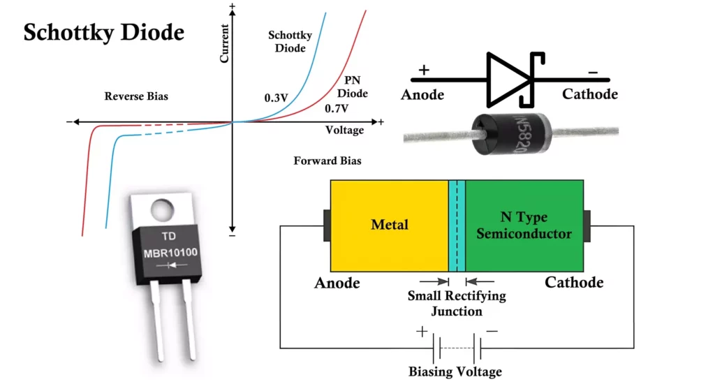
The symbol of a Schottky diode resembles that of a standard diode but includes a distinguishing characteristic. Instead of a simple straight line for the cathode, it features a thicker, bent line in S shape, indicating the metal-semiconductor junction. This differentiates it from the traditional p-n junction diode.

Construction of Schottky Diode
A Schottky diode is a type of semiconductor diode that has a lower forward voltage drop and faster switching speed compared to conventional diodes. Its construction is distinct from a standard p-n junction diode. Here’s a detailed explanation of its construction:
Basic Structure of a Schottky Diode
- Metal-Semiconductor Junction:
- The key difference in a Schottky diode is that it uses a metal-semiconductor junction instead of a p-n junction.
- On one side, a metal layer (e.g., aluminum, platinum, molybdenum, or gold) is deposited.
- On the other side, an n-type semiconductor material (usually silicon or gallium arsenide) is used.
- Layers in the Diode:
- Metal Layer (Cathode):
- This acts as the cathode and forms the metal-semiconductor junction.
- The metal chosen has specific work function properties to ensure good conduction with minimal voltage drop.
- N-Type Semiconductor Layer:
- The semiconductor layer is lightly doped n-type material that serves as the anode.
- This layer allows the formation of the Schottky barrier and supports current flow when forward-biased.
- Ohmic Contact:
- On the opposite side of the semiconductor, an ohmic contact is created to allow current to flow easily without additional barriers.
- Metal Layer (Cathode):
- Schottky Barrier:
- At the junction between the metal and the n-type semiconductor, a Schottky barrier forms due to the difference in work function between the metal and the semiconductor.
- This barrier controls the flow of charge carriers, leading to the unique properties of the diode, such as low forward voltage and fast switching.

Schottky Diode Construction

Construction Process
- Substrate Preparation: A thin wafer of n-type semiconductor is prepared with high crystalline purity.
- Metal Deposition: A thin layer of metal is deposited on the surface of the semiconductor using processes like sputtering, vacuum deposition, or chemical vapor deposition (CVD).
- Ohmic Contact Creation: On the opposite side of the semiconductor wafer, an ohmic contact is formed to provide a low-resistance path for current flow.
- Encapsulation: The device is encapsulated to protect it from environmental factors and to ensure stable operation.
Key Properties of a Schottky Diode
- Low Forward Voltage Drop: Typically, between 0.2V and 0.4V, compared to 0.7V for a silicon p-n junction diode.
- High Switching Speed: The absence of a depletion region eliminates charge storage, enabling faster switching.
- Limited Reverse Voltage: Schottky diodes usually have lower reverse breakdown voltages compared to p-n junction diodes.
- Higher Leakage Current: Due to the metal-semiconductor interface, leakage currents are higher than standard diodes.
VI Characteristics of Schottky Diode
The VI characteristics of a Schottky diode describe the relationship between its voltage (V) across the diode and the resulting current (I) flowing through it. Schottky diodes are unique due to their construction, which results in distinct characteristics compared to standard PN-junction diodes. Below is an explanation of these characteristics:
1. Forward Bias Region:
- Low Forward Voltage Drop:
A Schottky diode has a lower forward voltage drop (typically 0.2V to 0.45V) compared to a silicon PN-junction diode (~0.7V). This is because of the metal-semiconductor junction instead of the traditional PN junction. - Rapid Current Rise:
When the diode is forward-biased, current increases exponentially with a small increase in forward voltage. The equation governing forward current through diode is given as:I = Is (eqV/nkT − 1)
Where:
- Is: Reverse saturation current
- q: Charge of an electron
- V: Forward voltage
- n: Ideality factor (close to 1 for Schottky diodes)
- k: Boltzmann constant
- T: Absolute temperature
- High Current Handling:
Schottky diodes can handle high forward currents due to their lower resistance and reduced power loss.
Schottky Diode VI Characteristics

2. Reverse Bias Region:
- Low Reverse Breakdown Voltage:
Schottky diodes have a relatively low reverse breakdown voltage, typically ranging from 20V to 100V. Exceeding this voltage leads to a sharp increase in reverse current and diode damage. - Higher Reverse Leakage Current:
In the reverse bias, the diode has a higher leakage current compared to a standard diode. This is due to the tunneling effect at the metal-semiconductor junction. The leakage current increases with temperature.
3. Turn-On and Switching Characteristics:
- Faster Switching:
Schottky diodes exhibit extremely fast switching speeds due to the absence of charge storage in the depletion region (unlike PN diodes, which involve minority carriers). This makes them suitable for high-frequency applications like switching power supplies. - Low Turn-On Voltage:
The turn-on voltage (threshold voltage where current starts to flow significantly) is lower, making them energy-efficient in low-voltage applications.
4. Breakdown Region:
- When the reverse voltage exceeds the breakdown voltage, the diode conducts a large reverse current, leading to irreversible damage unless the diode is designed to operate in this region (Zener-like operation).
VI Characteristics Graph:
- Forward Bias (Quadrant I):
- Current rises exponentially after the turn-on voltage (0.2V–0.45V).
- Reverse Bias (Quadrant III):
- Minimal reverse current (leakage) initially.
- Sudden breakdown at the reverse voltage limit.
Working of Schottky Diode
The working of Schottky diode is based on movement of charge carriers across metal-semiconductor junction:
- Forward Bias (Positive voltage on anode):
- When the anode is more positive than the cathode, electrons in the n-type semiconductor gain enough energy to overcome the energy barrier at the metal-semiconductor interface.
- These electrons flow from the semiconductor to the metal, creating a current.
- Key Advantage: The voltage required for this to happen (forward voltage drop) is typically 0.2V to 0.4V, much lower than the 0.7V of standard silicon diodes.
- Reverse Bias (Positive voltage on cathode):
- When the cathode is more positive than the anode, the metal-semiconductor junction prevents most current from flowing.
- However, due to the nature of the junction, there is a small reverse leakage current caused by thermionic emission of electrons. This leakage is usually higher than that of a standard diode.
The absence of minority carrier injection (as in p-n junction diodes) leads to faster switching times, ideal for high-speed applications.
Schottky Transistor
A Schottky transistor is a type of bipolar junction transistor (BJT) designed with a built-in Schottky diode between the base and collector. The Schottky diode prevents the transistor from entering deep saturation by clamping the base-collector voltage to a low value (around 0.2–0.4V), improving switching speed.

Key Features of Schottky transistor:
- Prevention of Saturation: The Schottky diode ensures the transistor doesn’t fully saturate, reducing storage time.
- Faster Switching: Used in high-speed applications like digital circuits (e.g., TTL logic).
- Reduced Power Losses: Improved efficiency due to minimal storage charge.
In short, the Schottky transistor is optimized for speed and efficiency, making it ideal for high-frequency and digital switching applications.
Advantages of Schottky Diode
- Low Forward Voltage Drop (Vf):
- Typically, around 0.15–0.45V (compared to 0.6–0.7V in standard silicon diodes).
- Results in lower power losses and higher efficiency in circuits, especially at low voltage.
- High Switching Speed:
- Schottky diodes have minimal charge storage, enabling them to switch on and off rapidly.
- Ideal for high-frequency applications such as switching power supplies and RF circuits.
- Low Reverse Recovery Time:
- Unlike PN junction diodes, Schottky diodes have no significant minority carrier storage, leading to negligible reverse recovery time.
- This property is crucial in reducing switching noise and power losses in fast-switching circuits.
- Efficient at High Frequencies:
- Excellent for use in RF mixers, detectors, and other high-speed applications due to their small junction capacitance.
- Lower Heat Generation:
- The reduced forward voltage drop translates to less heat generation, improving thermal efficiency and reducing cooling requirements.
- Compact and Lightweight:
- Suitable for applications where size and weight constraints are critical.
Disadvantages of Schottky Diode
- Lower Reverse Voltage Rating:
- Schottky diodes typically have a lower reverse breakdown voltage (generally below 100V, though high-voltage versions exist).
- This limits their application in high-voltage circuits.
- Higher Leakage Current:
- Schottky diodes exhibit higher reverse leakage currents compared to standard silicon diodes, especially at elevated temperatures.
- This can lead to power losses in low-current or precision applications.
- Limited Temperature Tolerance:
- The performance of Schottky diodes deteriorates at higher temperatures due to increased leakage current.
- This makes them less suitable for high-temperature environments without additional thermal management.
- Cost:
- Schottky diodes are generally more expensive than standard silicon diodes, particularly in high-performance applications.
Applications of Schottky Diodes
Schottky diodes are widely used in energy-sensitive and high-frequency applications due to their unique characteristics, such as low forward voltage drop, fast switching speeds, and low reverse recovery time. Here are some common applications:
1. Power Rectification
- Low Voltage Rectifiers: Schottky diodes are used in power supplies, particularly for low-voltage applications, due to their low forward voltage drop (typically 0.15V to 0.45V).
- High-Efficiency Rectifiers: Used in DC-DC converters and AC-DC power supplies to minimize energy losses.
2. Switching Circuits
- High-Speed Switching: Their fast switching characteristics make them ideal for use in circuits requiring rapid transitions, such as digital circuits or pulse applications.
- Flyback Diodes: Used in inductive circuits (e.g., motors, relays) to suppress voltage spikes and protect components.
3. RF and Microwave Applications
- Mixer Diodes: Used in radio frequency (RF) and microwave systems as mixers in communication devices.
- Detector Diodes: Employed in RF detection and signal processing circuits due to their fast response time.
4. Clamping and Protection Circuits
- Voltage Clamping: Protects sensitive electronic circuits by clamping voltage surges and preventing overvoltage.
- Reverse Polarity Protection: Prevents damage to a circuit if the power supply is connected with the wrong polarity.
5. Solar Panel Systems
- Blocking Diodes: Prevents reverse current flow from the battery to the solar panel during nighttime or low-light conditions.
- Bypass Diodes: Protects individual solar cells from overheating when partially shaded.
6. Logic Circuits
- Low Voltage Drop in Logic Gates: Used in some low-power logic circuits where voltage drop minimization is critical.
- OR-Tying in TTL Circuits: Schottky diodes are used to “OR” outputs of multiple TTL circuits, ensuring minimal voltage drop.
7. Voltage Multipliers
- Used in circuits designed to step up DC voltages, such as in high-voltage power supplies or ionizer circuits.
8. Automotive Applications
- ECUs (Electronic Control Units): Used for fast, efficient rectification and clamping in automotive control circuits.
- Protection Circuits: Protect automotive electronics from voltage spikes caused by alternator switching or inductive loads.
9. Frequency Multiplication
- In RF applications, Schottky diodes are used to multiply frequencies for use in signal generation and communication systems.
Conclusion
The Schottky diode is an essential component in modern electronics, offering unique advantages like low forward voltage drop, high efficiency, and fast switching speeds. Despite its limitations, such as high reverse leakage current and low reverse voltage rating, it remains indispensable in applications ranging from power supplies to high-speed communication systems. Understanding its construction, working, and characteristics enables engineers to utilize it effectively in various applications.
Types of Diodes with Symbol, Definition, Working and Applications