In this article, we will explore the PIN diode in detail, covering its symbol, construction, VI characteristics, working principle, advantages, disadvantages, and applications.
A PIN diode is a type of semiconductor device that is widely used in RF and microwave applications. The name “PIN” comes from the structure of the diode, which consists of three layers: P-type, Intrinsic, and N-type semiconductor materials.
The intrinsic layer is the key feature that distinguishes the PIN diode from a standard PN junction diode. This intrinsic region is essentially undoped or lightly doped, which gives the PIN diode its unique properties, such as high-frequency operation, low capacitance, and high breakdown voltage.
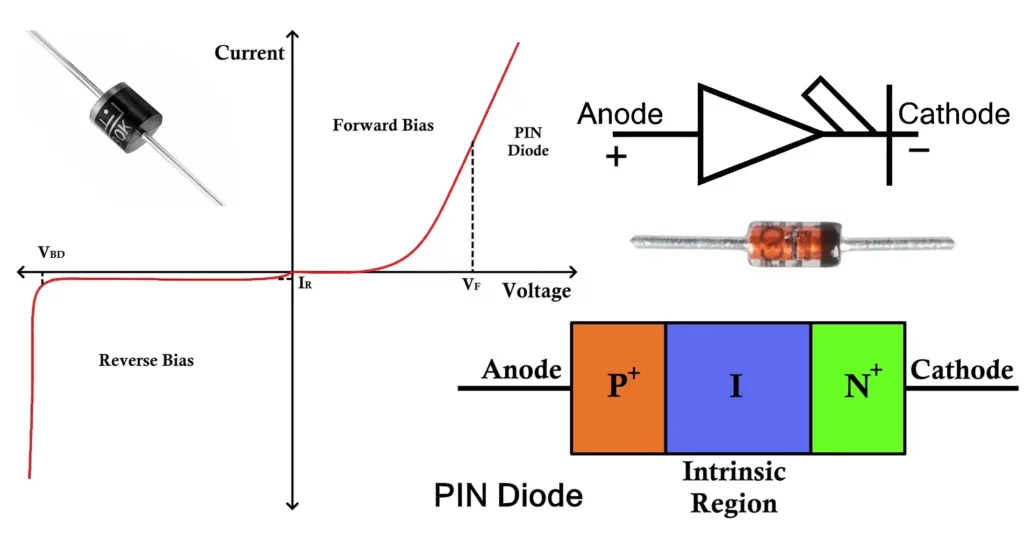
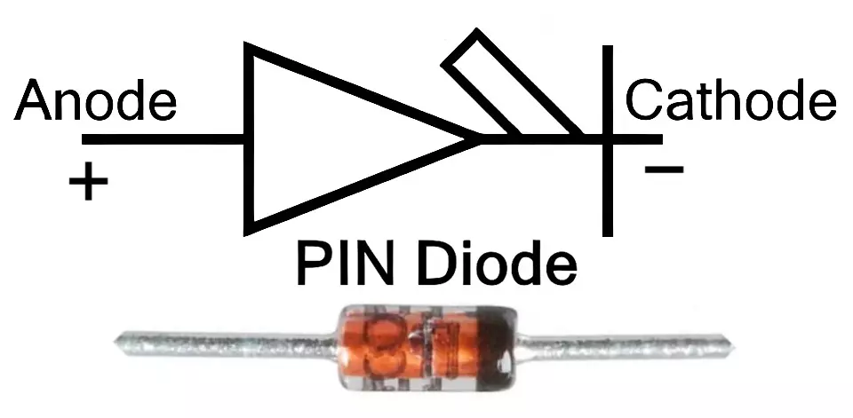
1. PIN Diode Symbol
The symbol of a PIN diode is similar to that of a standard PN junction diode but with a slight modification to represent the intrinsic region. The symbol consists of:
- An arrow pointing from the P-type material to the N-type material, indicating the direction of conventional current flow when the diode is forward-biased.
- Slanted lines representing the intrinsic (I) region between the P and N layers.
Here is the PIN diode symbol:
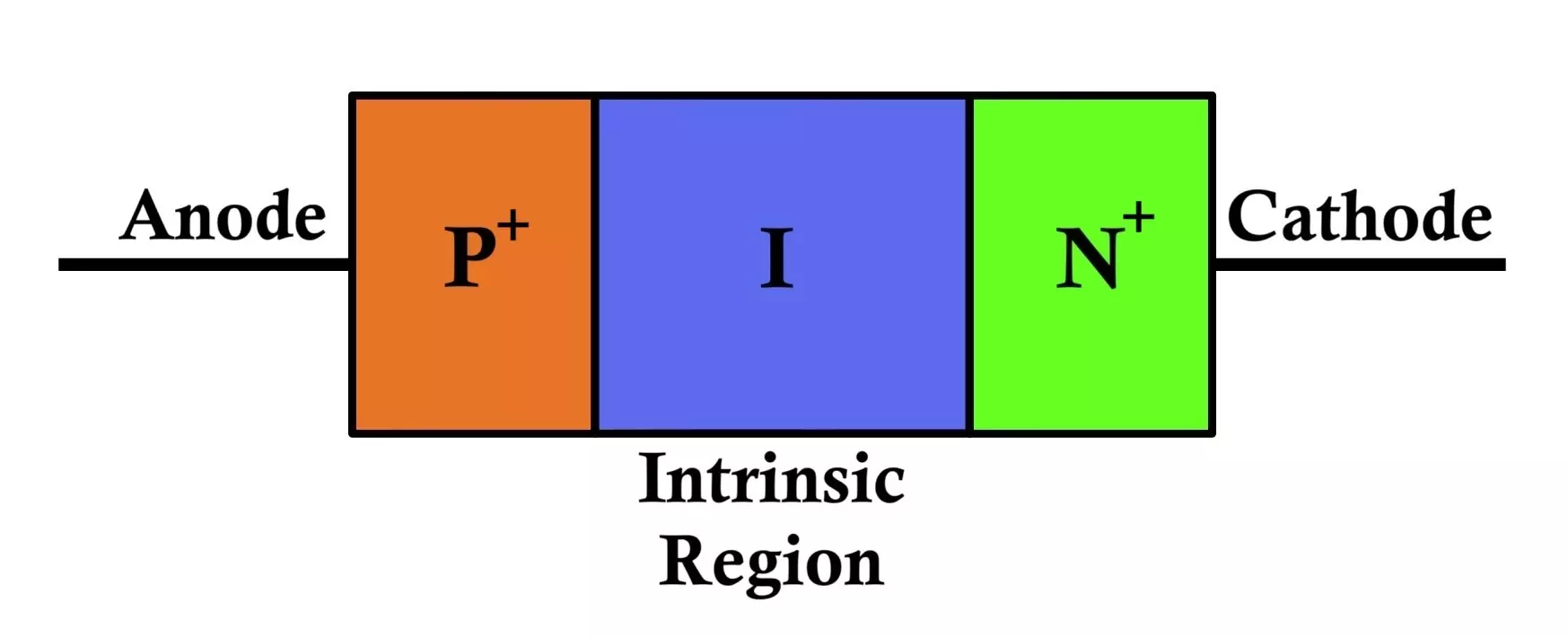
2. Construction of PIN Diode
The PIN diode is constructed using three layers of semiconductor material:
- P-type Layer: This layer is heavily doped with acceptor impurities (e.g., Boron) to create a high concentration of holes.
- Intrinsic Layer: This is the middle layer, which is either undoped or lightly doped. It acts as a spacer between the P and N layers and is responsible for the unique properties of the PIN diode.
- N-type Layer: This layer is heavily doped with donor impurities (e.g., Phosphorus) to create a high concentration of electrons.
The intrinsic layer is much wider than the P and N layers, which reduces the capacitance of the diode and allows it to operate at high frequencies. The overall structure is as follows:
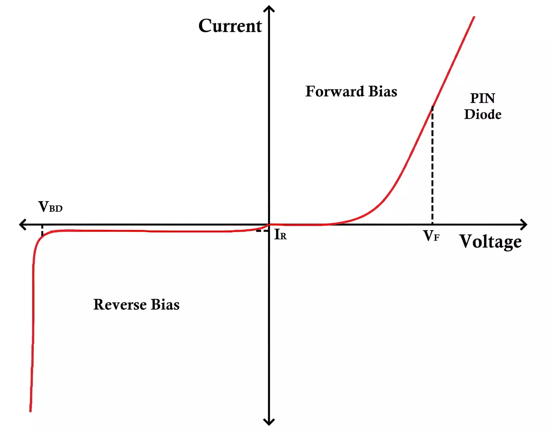
3. VI Characteristics of PIN Diode
The VI (Voltage-Current) characteristics of a PIN diode describe the relationship between the voltage applied across the diode and the resulting current. The VI curve of a PIN diode is similar to that of a standard PN junction diode but with some differences due to the intrinsic layer.
Forward Bias Condition:
- When a forward voltage is applied (positive voltage to the P-side and negative voltage to the N-side), the diode starts conducting.
- Initially, the current increases slowly due to the high resistance of the intrinsic region.
- As the voltage increases, the intrinsic region becomes flooded with charge carriers (holes and electrons), reducing its resistance and allowing a significant increase in current.
Reverse Bias Condition:
- When a reverse voltage is applied (positive voltage to the N-side and negative voltage to the P-side), the diode acts as a variable capacitor.
- The width of the depletion region increases, and the capacitance decreases.
- The reverse leakage current is very small due to the high resistance of the intrinsic layer.
The VI characteristics curve of a PIN diode is as shown:
4. Working of PIN Diode
The working of a PIN diode can be understood in two modes: forward bias and reverse bias.
No Bias Condition:
- The P-region has holes (positive charge carriers), and the N-region has electrons (negative charge carriers).
- The intrinsic layer has equal numbers of holes and electrons, making it neutral and acting as an insulator.
- No current flows through the diode.
Forward Bias Mode:
- When a forward voltage is applied, holes from the P-region and electrons from the N-region are injected into the intrinsic region.
- These charge carriers recombine in the intrinsic region, allowing current to flow through the diode.
- The intrinsic region acts as a low-resistance path, enabling the diode to conduct heavily.
Reverse Bias Mode:
- When a reverse voltage is applied, the depletion region widens, and the intrinsic region acts as an insulator.
- The diode behaves like a variable capacitor, with the capacitance depending on the width of the depletion region.
- The reverse leakage current is minimal, making the PIN diode suitable for high-frequency applications.
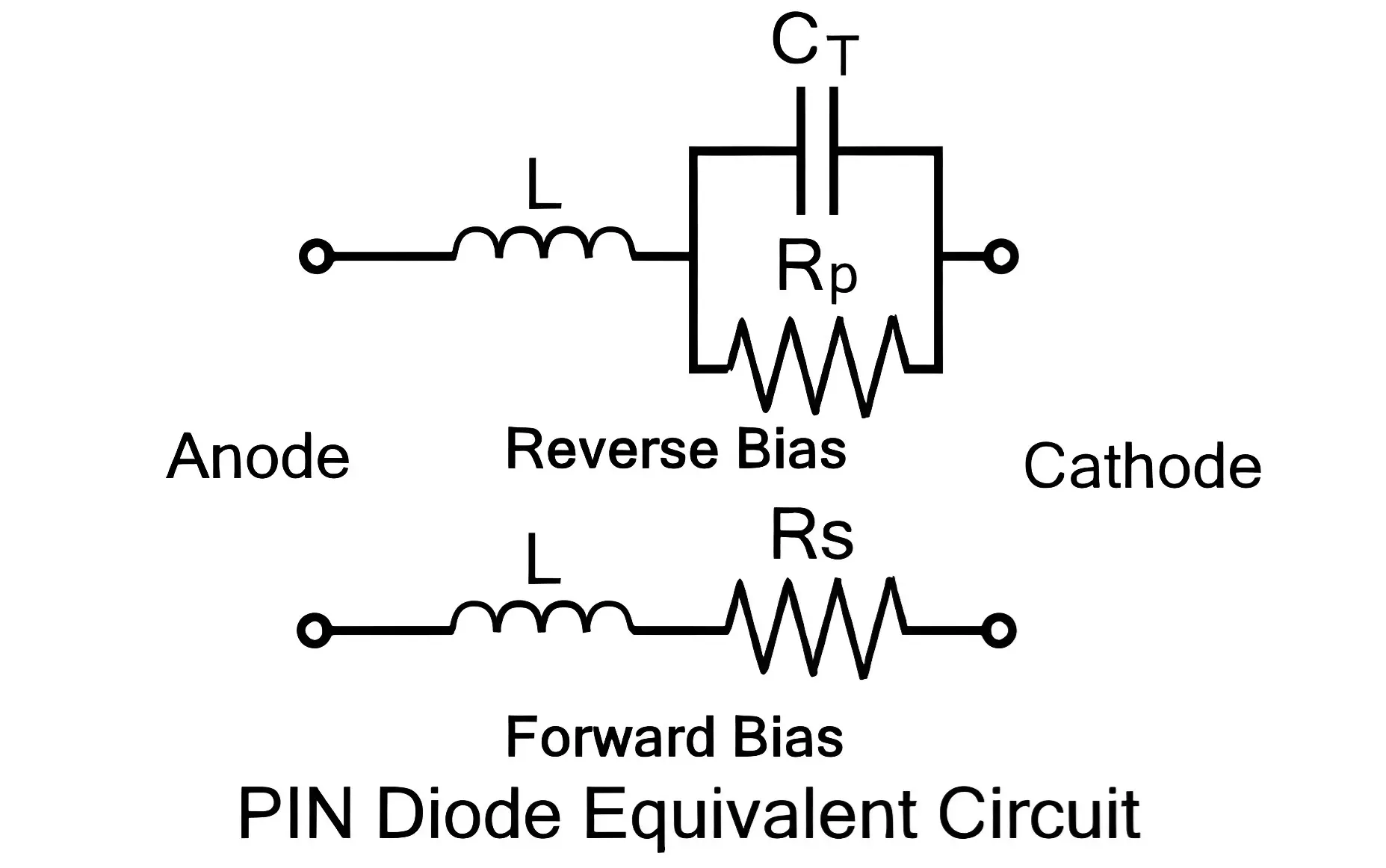
5. PIN Diode Equivalent Circuit
In forward bias, the PIN diode behaves like a variable resistor with a small parasitic inductance.
- The forward resistance (R) is low, typically in the range of a few ohms.
- The junction capacitance (C) is negligible because the intrinsic region is flooded with charge carriers.
- The parasitic inductance (L) is small but becomes significant at very high frequencies.
In reverse bias, the PIN diode behaves like a variable capacitor with a high resistance.
- The reverse resistance (R) is very high, typically in the range of megaohms (MΩ).
- The junction capacitance (C) is significant and depends on the width of the depletion region. It decreases with increasing reverse voltage.
- The parasitic inductance (L) remains the same as in forward bias.
The equivalent circuit of PIN diode in forward and reverse bias can be represented as:
6. Advantages of PIN Diodes
- High-Frequency Performance – The intrinsic layer reduces capacitance, allowing operation at microwave and RF frequencies.
- Fast Switching Speed – Ideal for RF and microwave switching applications.
- Low Noise – Used in low-noise signal applications, such as RF receivers.
- High Power Handling – Can handle large RF power without significant signal distortion.
- Good Linearity – Suitable for RF attenuators and modulators.
- Efficient Photodetection – Used in photodiodes for optical communication.
- Low Reverse Recovery Time – Useful in high-speed rectification applications.
- Controlled Resistance – Acts as a variable resistor in RF circuits.
7. Disadvantages of PIN Diodes
- Higher Forward Voltage Drop – Requires more power than standard diodes.
- Limited Low-Frequency Performance – Less efficient at lower frequencies due to its wide depletion region.
- Temperature Sensitivity – Performance varies with temperature changes.
- Complex Biasing Requirements – Needs a proper DC bias circuit for optimal operation.
- Higher Manufacturing Cost – More expensive than standard p-n junction diodes.
- Limited Current Capability – Not suitable for applications requiring high current conduction.
8. Applications of PIN Diodes
- RF and Microwave Switching – Used in high-frequency RF switches and phase shifters.
- Attenuators – Provides variable attenuation in RF circuits.
- RF Modulators and Demodulators – Used in communication systems for signal processing.
- Photodetectors – Functions as a photodiode in fiber-optic communication and light sensors.
- High-Speed Rectification – Used in fast recovery rectifiers for power electronics.
- Antenna Switching – Employed in radar and communication systems.
- Medical Imaging – Found in X-ray and MRI systems for signal detection.
- Automotive Radar – Used in adaptive cruise control and collision detection systems.
- Satellite and Aerospace – Utilized in RF and microwave communication for space applications.
- Military and Defense – Applied in electronic warfare and radar jamming systems.
Conclusion
The PIN diode is a versatile semiconductor device that plays a crucial role in modern electronics, especially in high-frequency and RF applications. Its unique construction, with an intrinsic layer sandwiched between P and N layers, gives it distinct advantages such as low capacitance, high breakdown voltage, and fast switching speed. While it has some limitations, such as a higher forward voltage drop and complex construction, its benefits far outweigh the drawbacks in many applications.
From RF switches and attenuators to photodetectors and phase shifters, the PIN diode continues to be an essential component in advanced electronic systems. Understanding its symbol, construction, VI characteristics, working principle, and applications is key to leveraging its capabilities in designing efficient and high-performance circuits.
Types of Diodes with Symbol, Definition, Working and Applications