Engineers and designers widely use a buck converter circuit, also known as a step-down converter, to efficiently reduce a higher input voltage to a lower output voltage while maintaining high efficiency. They commonly use it in power supplies, battery chargers, electric vehicles, and embedded systems.
Buck Converter Circuit Diagram
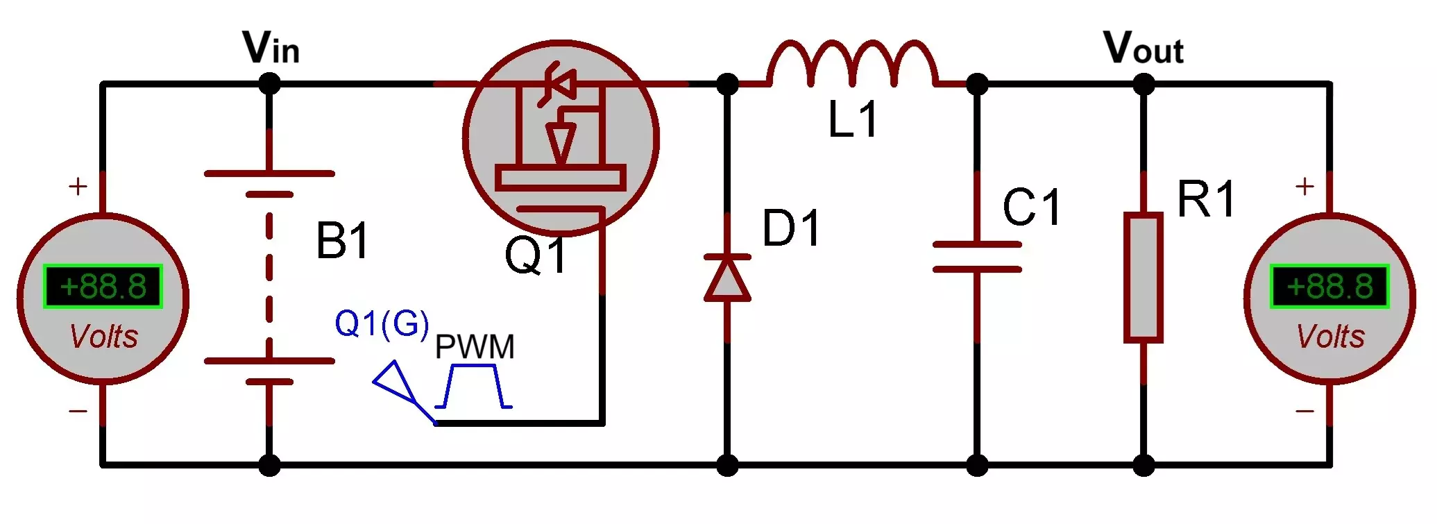
Below is a typical Buck Converter Circuit:
Components Used
| Component | Description |
|---|---|
| B1 | DC power source (Battery or other input supply) |
| Q1 | Power MOSFET switch, controlled by PWM signal |
| D1 | Flyback/freewheeling diode (typically fast recovery or Schottky) |
| L1 | Inductor for energy storage and smoothing |
| C1 | Output capacitor for filtering |
| R1 | Load resistor (represents the connected load) |
Construction of Buck Converter
The buck converter circuit can be broken into four key sections:
1. Input Section (B1 and Q1)
- B1 supplies a higher DC voltage.
- Q1, a MOSFET, acts as a high-speed switch. Its gate is driven by a PWM (Pulse Width Modulation) signal. By adjusting the duty cycle of the PWM, the average output voltage is controlled.
2. Freewheeling Path (D1)
- The diode D1 provides a path for inductor current when Q1 is turned OFF. This maintains continuous current flow and prevents voltage spikes.
3. Energy Storage & Filtering (L1 and C1)
- The inductor L1 stores energy when Q1 is ON and releases it when Q1 is OFF.
- The capacitor C1 smooths out voltage ripples, providing a steady DC output.
4. Load (R1)
- The load resistor R1 simulates a connected device or circuit drawing current from the buck converter.
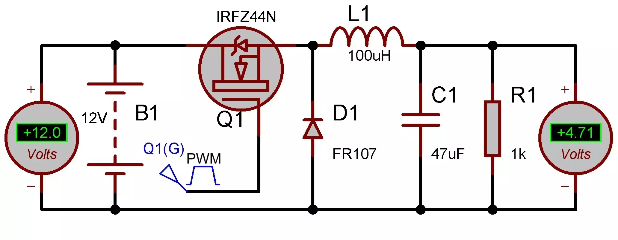
Here is a simple buck converter circuit stepping down 12 DC to 4.7V DC.
Working of Buck Converter (Step-by-Step)
The buck converter works in two main phases based on the ON/OFF state of the MOSFET Q1:
Mode 1: MOSFET ON (PWM High)
- The MOSFET Q1 conducts, connecting the input voltage directly across the inductor L1 and the load.
- The inductor stores energy in the form of a magnetic field.
- The output voltage rises and powers the load.
- Diode D1 is reverse-biased and does not conduct.
Inductor current increases during this time.
Mode 2: MOSFET OFF (PWM Low)
- The MOSFET turns off, breaking the path from the battery.
- The inductor resists sudden change in current, so it releases energy.
- The diode D1 conducts, providing a return path for inductor current.
- The inductor supplies energy to both the load and recharges capacitor C1.
- Output voltage decreases slightly.
Inductor current decreases, but flow remains continuous.
Voltage Output Formula
The average output voltage Vout is related to the input voltage Vin by the PWM duty cycle DD (ON time as a fraction of total cycle):
Vout = D × Vin
Where:
- D = Ton/Ton + Toff
- Vin = Input DC voltage
- Vout = Output voltage across the load
This makes the buck converter voltage-controllable by adjusting the PWM signal.
Need of Feedback in Buck Converter Circuit
The output voltage of a buck converter can change with varying load, and that’s why feedback control is essential for voltage stability in practical designs.
Why Output Voltage Changes with Load:
Without feedback, the converter is open-loop, and the output voltage depends on:
- The PWM duty cycle (fixed or manually set).
- The load current — as the load increases (i.e., R1 decreases), the voltage across the load can drop due to:
- Voltage ripple.
- Inductor’s internal resistance.
- Drop across the diode and MOSFET.
- Insufficient energy being transferred during the PWM ON time.
Why Feedback is Needed:
In closed-loop control, a feedback circuit continuously samples the output voltage and adjusts the PWM duty cycle to keep the output stable.
Typical Feedback Loop:
- A voltage divider steps down the output voltage.
- An error amplifier (often part of a PWM controller IC) compares it to a reference voltage.
- The PWM signal is adjusted accordingly to regulate the output.
Benefits of Feedback:
- Maintains constant voltage despite varying load or input voltage.
- Enables fast transient response to sudden load changes.
- Protects connected devices from over-voltage or under-voltage.
- Essential for regulated power supplies and precision electronics.
Note: The output voltage can drop under load in an open-loop buck converter. Voltage feedback to the PWM controller is necessary to maintain a stable and accurate output voltage in real-world applications.
Advantages of Buck Converter
| Advantage | Explanation |
|---|---|
| High Efficiency | Typically 85–95% because power loss is minimal in switching devices. |
| Compact Size | Requires smaller heat sinks and components compared to linear regulators. |
| Precise Control | Output voltage can be finely tuned by changing the PWM duty cycle. |
| Scalability | Can handle a wide range of input/output voltage levels and currents. |
| Low Heat Generation | Unlike linear regulators, very little power is dissipated as heat. |
Disadvantages of Buck Converter
| Disadvantage | Explanation |
|---|---|
| Complex Design | Requires careful design of switching frequency, control loop, and components. |
| Electromagnetic Interference (EMI) | High-speed switching can produce noise and EMI. |
| Inductor Size | Inductors may be bulky for high current applications. |
| Output Ripple | Output voltage contains ripple if not filtered properly. |
| Needs Fast Diode | Requires a low forward voltage drop, fast-recovery or Schottky diode. |
Applications of Buck Converter
| Application | Use Case |
|---|---|
| Battery-Powered Devices | Efficient voltage regulation in smartphones, tablets, laptops. |
| Embedded Systems | Supplies lower voltages to microcontrollers and sensors. |
| LED Drivers | Regulates current in LED lighting systems. |
| Automotive Electronics | Steps down car battery voltage (12V/24V) to logic-level voltages. |
| Solar Power Systems | MPPT controllers and voltage regulators in PV systems. |
| Industrial Automation | Powering sensors, PLCs, and control modules from higher voltages. |
| DC Motor Drives | Controls the speed of DC motors by varying voltage. |
Tips for Designing a Buck Converter
- Use low Rds(on) MOSFETs for high efficiency.
- Choose low ESR capacitors to minimize output ripple.
- Use Schottky diodes for fast switching and low forward drop.
- Size the inductor properly to prevent saturation and maintain continuous conduction.
- Implement feedback control for regulated output.
- Include input and output filters to reduce noise and EMI.
Most Commonly Used Buck Converter ICs
For better regulation, control and efficiency we generally use buck converter ICs instead of using a lot of external components. Here are some of the most commonly used buck converter ICs across various applications:
1. Texas Instruments (TI)
- LM2596 – A classic, widely-used step-down regulator (up to 3A).
- TPS5430 / TPS54160 – Synchronous buck converters for higher efficiency.
- LM2937 / LM2940 – Low-dropout regulators with buck-like behavior.
2. Analog Devices (including Linear Technology)
- LT1763 / LT8610 / LT8609 – High-performance, low-noise buck converters.
- LTC3600 – Precision buck regulator with very low dropout.
3. Microchip (including Microsemi)
- MIC2205 / MIC4680 – Compact buck regulators suitable for portable devices.
- MCP16301 – Efficient buck converter for up to 600mA.
4. STMicroelectronics
- L4971 / L7985A – Robust converters for industrial and automotive use.
- ST1S10 – Small, efficient buck converter for consumer electronics.
5. ON Semiconductor
- NCP3065 / NCP buck series – Popular in LED drivers and power supplies.
- NCP3170 – High-current buck regulator (3A).
6. Maxim Integrated (now part of Analog Devices)
- MAX5035 / MAX17503 – High-voltage buck converters.
- MAX16990 – Automotive-grade buck controller IC.
These ICs vary in terms of input/output voltage range, current capability, switching frequency, and packaging, making them suitable for different applications – from mobile devices to automotive and industrial systems.
Conclusion
A buck converter is an essential building block in modern power electronics, allowing efficient voltage conversion in a compact form. Understanding its circuit, working principles, and design considerations enables engineers and hobbyists to build robust power supplies for various applications.
It’s a perfect example of how switching electronics can outperform traditional linear methods in both efficiency and flexibility.